A method for phase change memory cell integration using electrochemical deposition

A technology using electrochemistry and phase change storage, applied in electrical components and other directions, can solve problems such as clogging of filling methods, and achieve the effects of easy operation, good contact, and low requirements for experimental conditions

Active Publication Date: 2021-09-28
HUAZHONG UNIV OF SCI & TECH
View PDF4 Cites 0 Cited by
  • Summary
  • Abstract
  • Description
  • Claims
  • Application Information

AI Technical Summary

Problems solved by technology

[0005] Aiming at at least one of the above defects or improvement needs of the prior art, especially the clogging problem existing in the existing filling method, the present invention provides a method for reusing deep holes with nanoscale apertures etched by micro-nano processing technology. The method of electrochemical deposition is a process method for quickly and effectively filling deep holes, which can grow nano-phase change materials from the bottom of nano-pores, and can realize the filling of chalcogenide phase-change materials with multi-layer and complex structures in small holes with ultra-large aspect ratios.

Method used


Image

  • A method for phase change memory cell integration using electrochemical deposition
  • A method for phase change memory cell integration using electrochemical deposition
  • A method for phase change memory cell integration using electrochemical deposition

Examples


specific Embodiment approach

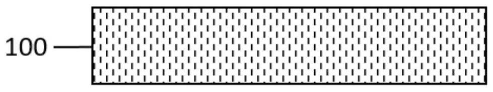
[0069] Place the silicon wafer in acetone and alcohol for ultrasonic cleaning for about ten minutes; after the ultrasonic is completed, use a nitrogen gun to blow off the residual liquid on the surface and dry it for use.

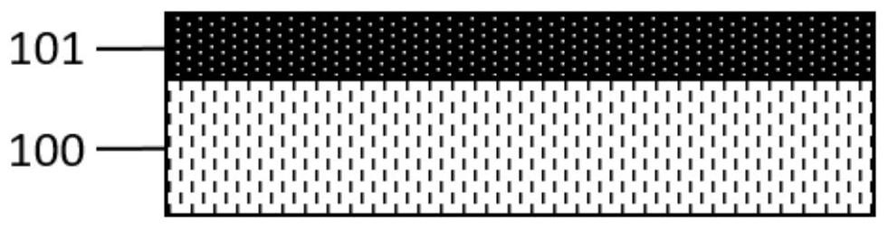
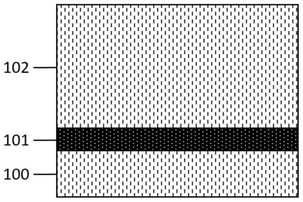
[0070] Use magnetron sputtering or electron beam evaporation to evaporate a metal conductive layer such as titanium platinum, nickel gold, etc. on a clean silicon wafer, with a thickness between 10nm and 200nm. Use PECVD or ALD to grow a layer of dense silicon dioxide or alumina. This step involves a high reaction temperature, but there is no functional layer on the sample, which will not affect the performance of the device. The thickness can reach the micron level or more according to the design requirements.

[0071] Combined with photolithography or other mask processes, the pattern is transferred to the sample. Use the etching method to etch small holes. If the depth of subsequent etching is deeper, the mask can be replaced with a mask that is more re...


PUM

PropertyMeasurementUnit
pore sizeaaaaaaaaaa
thicknessaaaaaaaaaa
thicknessaaaaaaaaaa

Abstract

The invention discloses a method for integrating phase-change storage units by using electrochemical deposition, comprising the steps of: S1: preparing a conductive substrate; S2: preparing an insulating layer; S3: preparing deep holes; S4: configuring a reaction solution, which is mixed with Two different electrolytes; S5: Electrochemical deposition is carried out from the bottom up in the deep hole. By adjusting the deposition parameters, the upper and lower layers of materials are deposited in the deep hole, namely the gating tube and the phase change unit; S6: Prepare the upper electrode . The deep hole with nanoscale aperture is etched by micro-nano processing technology, and then the electrochemical deposition method is used to quickly and effectively fill the deep hole. The nano phase change material can be grown from the bottom of the nanopore, which can achieve a super large aspect ratio. The small holes are filled with chalcogenide phase change materials with multi-layer complex structures. The precise control of material growth can be realized by adjusting the deposition parameters. The patterned growth can be realized by designing the electrode shape with potential applied at the bottom, and various complex structures can be realized. Preparation of materials.

Description

technical field [0001] The invention belongs to the technical field of microelectronic devices and memories, and in particular relates to a method for integrating phase-change memory units by using electrochemical deposition. Background technique [0002] The traditional phase-change memory (PCM) has gradually been unable to meet the demand for high-capacity storage in the era of big data. Whether it is the three-dimensional stacking of PCM or the continuous reduction of device size, it is to improve storage density and reliability. However, with the advancement of process nodes, not only the continuous increase of the aspect ratio of the device structure makes it difficult to fill deep holes in the process, but also the co-integration of the gate unit and the phase change material unit in the 3D Xpoints structure also depends on Fast and efficient deep hole filling process. [0003] Although advanced photolithography processes can carve nano-aperture patterns, commonly use...

Claims


Application Information

Patent Timeline
Patent Type & Authority Patents(China)
IPC IPC(8): H01L45/00
CPCH10N70/231H10N70/021H10N70/011H10N70/023
Inventor 徐明徐开朗缪向水童浩万代兴
Owner HUAZHONG UNIV OF SCI & TECH
Why Eureka
Try Eureka