Method for adding solder resist bridge between narrow IC pads on thick copper PCB

A technology for PCB boards and solder bridges, applied in the field of printed circuit boards, can solve problems such as reducing production costs, and achieve the effects of reducing solder short circuits and improving yields

Inactive Publication Date: 2020-04-17
WUS PRINTED CIRCUIT (KUNSHAN) CO LTD
View PDF3 Cites 1 Cited by
  • Summary
  • Abstract
  • Description
  • Claims
  • Application Information

AI Technical Summary

Problems solved by technology

[0004] In order to solve the deficiencies of the prior art, the present invention provides a method of adding a solder-rejection bridge between the narrow and small IC pads on the thick copper PCB by using the existing equipment, so as to reduce the number of thick copper PCBs with narrow and small IC pads. Solder short circuit problem that may occur during SMT assembly, while reducing production cost input

Method used


Image

  • Method for adding solder resist bridge between narrow IC pads on thick copper PCB
  • Method for adding solder resist bridge between narrow IC pads on thick copper PCB
  • Method for adding solder resist bridge between narrow IC pads on thick copper PCB

Examples


Embodiment Construction

[0020] The present invention will be further described below in conjunction with the accompanying drawings. The following examples are only used to illustrate the technical solution of the present invention more clearly, but not to limit the protection scope of the present invention.

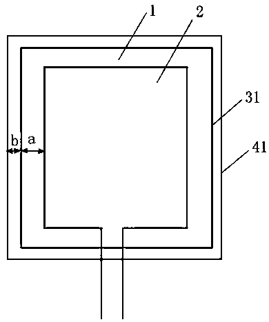
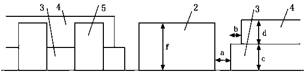
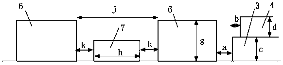
[0021] A method of adding solder-rejection bridges between narrow and small IC pads on a thick copper PCB:

[0022] Step 1. Create the outer layer circuit of single, double, or multilayer printed circuit board (PCB board), the thickness of the outer layer circuit is 25 microns to 125 microns, including copper lines and copper pads, etc., and the PCB board The distance between adjacent IC pads is greater than or equal to 150 microns;

[0023] Step 2: Use screen printing to print the first layer of ink on the surface of the PCB and pre-bake it; the thickness of the first layer of ink is from 25 microns to 65 microns (measured from the substrate);

[0024] Step 3: Use the photosensitive film imag...


PUM

PropertyMeasurementUnit
thicknessaaaaaaaaaa
thicknessaaaaaaaaaa
widthaaaaaaaaaa

Abstract

The invention discloses a method for adding a solder resist bridge between narrow IC pads on a thick copper PCB, and belongs to the technical field of printed circuit boards. The method comprises thefollowing steps: manufacturing an outer layer circuit of the PCB; printing a first layer of ink on the surface of the PCB with the outer layer circuit; carrying out exposure and development on the first layer of ink, and exposing places which do not need to be covered with the ink and not reserving the ink between the adjacent IC pads to form first solder resist windowing; printing a second layerof ink on the surface of the PCB with the outer layer circuit; exposing and developing the second layer of ink, forming a solder resist bridge and forming second solder resist windowing, wherein the size of the second solder resist windowing is greater than that of the first solder resist windowing; and baking until the ink is completely cured. The solder resist bridge of a relatively thin thickness is manufactured under the condition that the thick copper wire section can be covered by enough thick solder resist ink so that the solder resist bridge can stand stably in a narrow IC interval andcannot pollute IC pads on two sides; and the problem of solder short circuit caused by excessively narrow IC pads can be reduced so that the yield of SMT assembly is improved.

Description

technical field [0001] The invention belongs to the technical field of printed circuit boards, and in particular relates to a method for adding solder-rejection bridges between narrow and small IC pads on a thick copper PCB. Background technique [0002] The application of screen screen printing solder repelling ink and then film exposure and development is the most commonly used and low-cost and high-flexibility main production method for printed circuit boards (PCB boards). In addition, adding a solder maskdam between IC pads (integrated circuit pads) to prevent soldering short circuits is also a common and effective method to improve the assembly yield of SMT (surface mount technology) parts. With the development of science and technology, the design of electronic products has more functions, power consumption and heat generation increase, and more and more products are designed as thick copper; and because the finished product is smaller, the size of the parts is also re...

Claims


Application Information

Patent Timeline
Patent Type & Authority Applications(China)
IPC IPC(8): H05K3/34H05K3/00
CPCH05K3/0073H05K3/34
Inventor 陈家辉
Owner WUS PRINTED CIRCUIT (KUNSHAN) CO LTD
Why Eureka
Try Eureka