


Quick Research
Generate reliable direction feasibility study reports for your R&D in just a few steps.

Technical Q&A
Discover and master advanced knowledge NOW. Basics, ideas, possibilities, all at once.

Find Solutions
As an expert in R&D theories, this can generate solutions to your technical problems instantly.

Evaluate Feasibility
Analyze your overall solution with one click, know your potential R&D risks in advance.

Monitor Landscape
Get weekly tech updates, stay abreast of the latest tech innovations and key insights.
Coated PC composite board and manufacturing process thereof
A technology of composite board and first niobium oxide, which is applied in metal material coating process, sputtering plating, ion implantation plating, etc., can solve the problems of high cost, low production capacity, high requirements of coating process, etc., and achieve optimal attachment Focus on the effect
- Summary
- Abstract
- Description
- Claims
- Application Information
AI Technical Summary
Problems solved by technology
Method used
Image

Examples
Embodiment 1
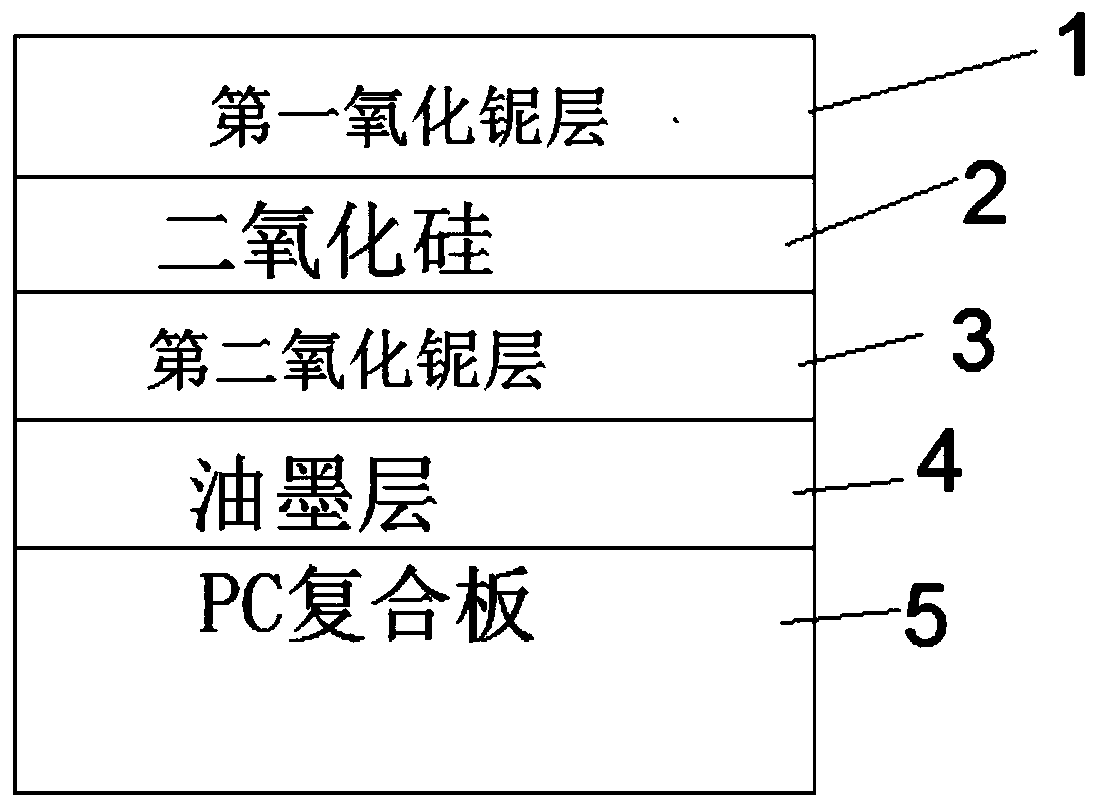
[0019] A coated PC composite board comprises, from top to bottom, a first niobium oxide layer, a silicon dioxide layer, a second niobium oxide layer, an ink layer and a PC composite board.
[0020] Further, the thickness of the first niobium oxide layer is 58nm.
[0021] Further, the thickness of the silicon dioxide layer is 25nm.
[0022] Further, the thickness of the second niobium oxide layer is 38nm.
[0023] A kind of preparation technology of the PC composite board of described coating comprises the following processing steps:
[0024] Step 1: Install the niobium oxide target and silicon dioxide target in the coating box, close the box, raise the temperature to 250°C, bake the coating box for 1.5 hours, and continuously vacuumize the box to remove the Water vapor and miscellaneous gases;
[0025] Step 2, wait until the local vacuum reaches 5×10 -4 Pa, filled with argon and oxygen with a purity of 99.99%, so that the working pressure reaches 0.5Pa;
[0026] Step 3, t...
Embodiment 2
[0028] A coated PC composite board comprises, from top to bottom, a first niobium oxide layer, a silicon dioxide layer, a second niobium oxide layer, an ink layer and a PC composite board.
[0029] Further, the thickness of the first niobium oxide layer is 53nm.
[0030] Further, the thickness of the silicon dioxide layer is 23nm.
[0031] Further, the thickness of the second niobium oxide layer is 35nm.
[0032] A kind of preparation technology of the PC composite board of described coating comprises the following processing steps:
[0033] Step 1: Install the niobium oxide target and silicon dioxide target in the coating box, close the box, raise the temperature to 280°C, bake the coating box for 1 hour, and continuously vacuum to remove the water in the box steam and fumes;
[0034] Step 2, wait until the local vacuum reaches 5×10 -4 Pa, filled with argon and oxygen with a purity of 99.99%, so that the working pressure reaches 0.6Pa;
[0035] Step 3, turn on the ion so...
PUM
| Property | Measurement | Unit |
|---|---|---|
| Thickness | aaaaa | aaaaa |
| Thickness | aaaaa | aaaaa |
| Thickness | aaaaa | aaaaa |
Abstract
Description
Claims
Application Information
 - R&D Engineer
- R&D Manager
- IP Professional
- Industry Leading Data Capabilities
- Powerful AI technology
- Patent DNA Extraction
Browse by: Latest US Patents, China's latest patents, Technical Efficacy Thesaurus, Application Domain, Technology Topic, Popular Technical Reports.
© 2024 PatSnap. All rights reserved.Legal|Privacy policy|Modern Slavery Act Transparency Statement|Sitemap|About US| Contact US: help@patsnap.com