An In Situ Controllable Bonding Method of Amorphous Nanowires and Porous Films

A technology of porous film and nanowire, applied in the direction of nanotechnology, nanotechnology, nanostructure manufacturing, etc., to achieve the effect of strong high-precision characteristics, strong flexibility and controllability

Active Publication Date: 2020-09-22
CHANGZHOU UNIV
View PDF13 Cites 0 Cited by
  • Summary
  • Abstract
  • Description
  • Claims
  • Application Information

AI Technical Summary

Problems solved by technology

However, with regard to the bonding or interconnection technologies between nanowires and thin films, in the existing literature, more nanowires are self-assembled and grown on the surface of the substrate through the "bottom-up" method. The wire itself; and there is no relevant report on the in-situ, flexible and controllable, high-precision, low-temperature bonding technology between the nanowire and the film through an artificial "top-down" method

Method used


Image

  • An In Situ Controllable Bonding Method of Amorphous Nanowires and Porous Films
  • An In Situ Controllable Bonding Method of Amorphous Nanowires and Porous Films
  • An In Situ Controllable Bonding Method of Amorphous Nanowires and Porous Films

Examples


Embodiment 1

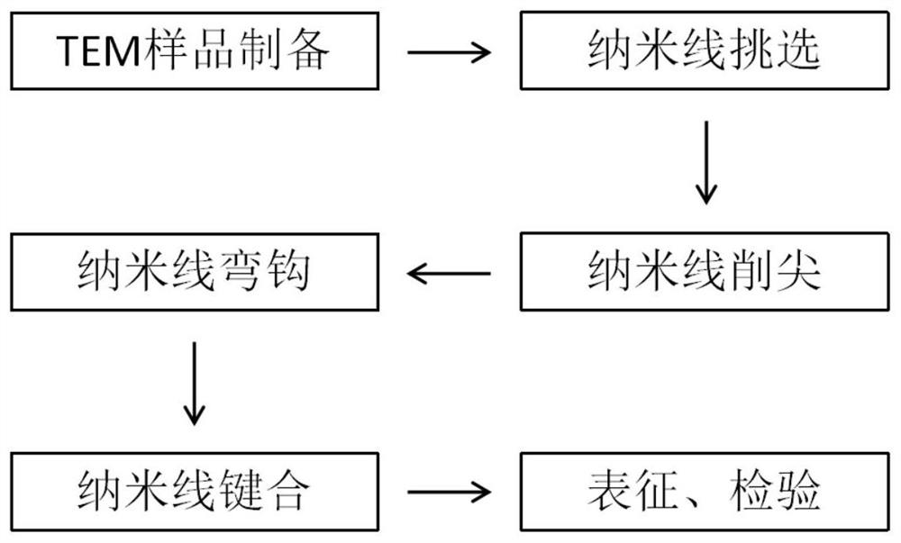
[0027] Example 1: Brittle amorphous SiO x Bonding of Nanowires and Porous Carbon Films with TEM Microgates

[0028] 1) TEM sample preparation:

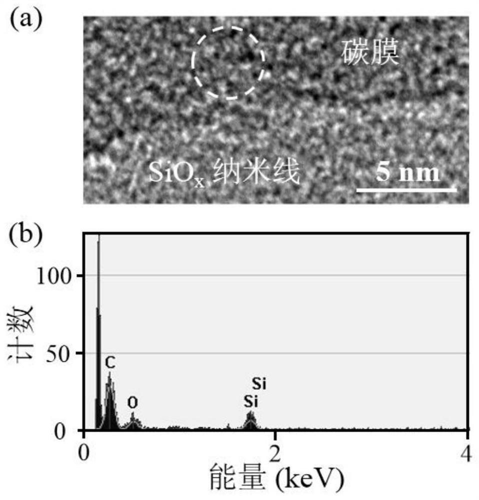
[0029] Scrape off a little SiO from the silicon wafer substrate with a blade x Nanowire powder (x Drop 2 drops of the ethanol solution of the nanowires onto the porous carbon film with a copper grid micro-grid. The pore diameter of the porous carbon film is about 1000 nm, and the TEM sample is obtained after standing for 15 minutes to dry.

[0030] 2) Nanowire screening:

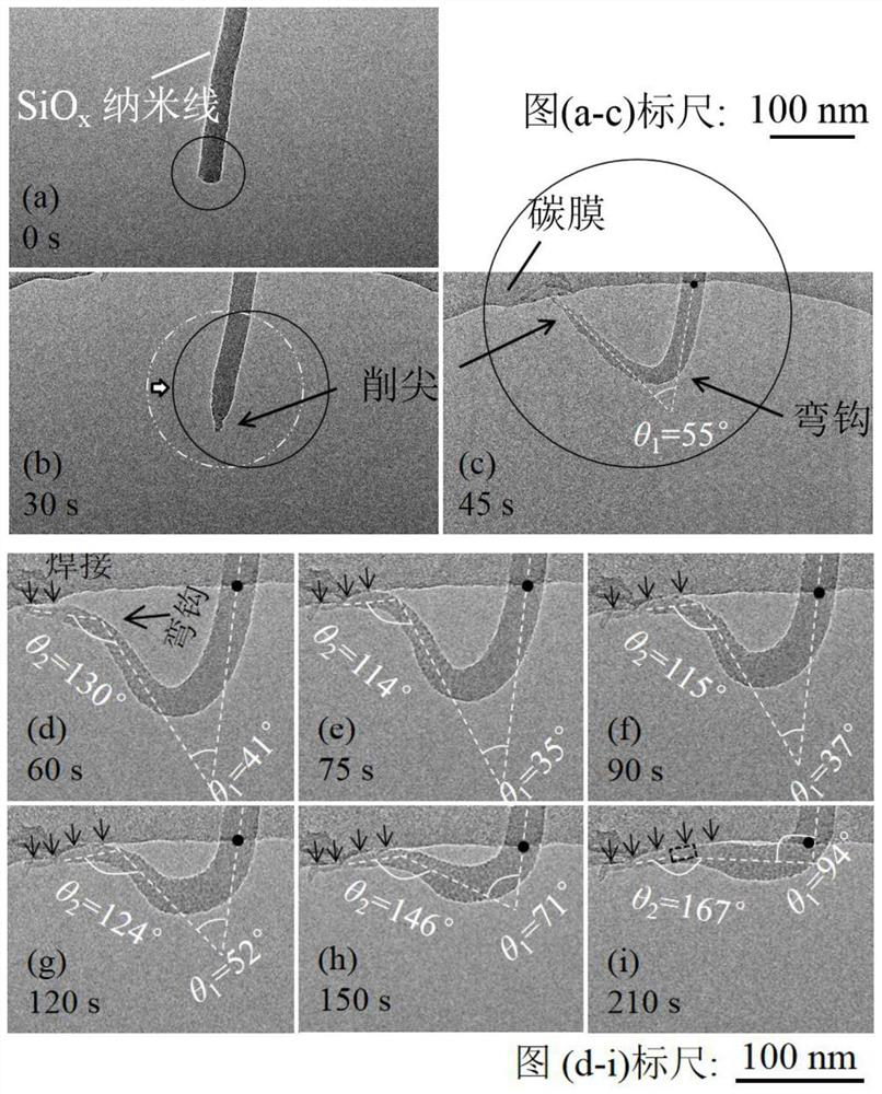
[0031] Load the TEM sample into a JEOL JEM-2100 transmission electron microscope with an accelerating voltage of 200kV, and then select the nanowire segment to be irradiated. Such as figure 2 As shown in (a), the nanowire segment contains free ends, and the free ends protrude into the pores of the porous carbon film; the TEM observation magnification of 50,000× is appropriate, and the overall morphology and main details of the nanowire segment can be observed a...


PUM

PropertyMeasurementUnit
pore sizeaaaaaaaaaa
sizeaaaaaaaaaa
current densityaaaaaaaaaa

Abstract

The invention discloses an in-situ controllable bonding method of amorphous nano-wires and a porous film. The method comprises: dispersing nano-wires on a transmission electron microscope (TEM) samplewith a porous film structure, putting the TEM sample into a TEM, selecting the nano-wire fragments with free ends projecting into the holes of the porous film, and carrying out bonding treatment under the observation of the TEM according to a process of nano-wire sharpening, nano-wire hooking and nano-wire bonding. According to the invention, based on the targeted irradiation of the high-energy electron beams in the transmission electron microscope, the amorphous nano-wires are sharpened and hooked, and the sharpened and hooked amorphous nano-wires are integrally bonded with the porous film in a high-quality mode, so the method has advantages of in-situ, flexible, controllable, high-precision and low-temperature bonding and the like.

Description

technical field [0001] The invention belongs to the field of micro-nano material processing, and in particular relates to an in-situ controllable bonding method of amorphous nanowires and porous films. Background technique [0002] Broadly speaking, bonding technology is a technology that bonds together through a chemical reaction at the interface between two materials. Bonding technology is widely used in the fields of MEMS devices and integrated circuits IC. It is a dynamic high-tech and is of great significance to the development of new technologies in our country. In MEMS and microelectronics manufacturing, bonding technology has become one of the important processes in micromachining, and it is an important part of microsystem and IC system packaging technology. At present, with the gradual increase in the integration of MEMS and microelectronic circuits, it is further required to realize its controllable bonding technology in a smaller nanoscale range, or to be able t...

Claims


Application Information

Patent Timeline
Patent Type & Authority Patents(China)
IPC IPC(8): B82B3/00B82Y40/00
CPCB82B3/0047B82Y40/00
Inventor 苏江滨吉高峰王智伟马骥何祖明唐斌蒋美萍
Owner CHANGZHOU UNIV
Why Eureka
Try Eureka