Gridding photovoltaic backboard and preparation method thereof
A photovoltaic backplane, grid technology, applied in photovoltaic power generation, final product manufacturing, sustainable manufacturing/processing, etc., can solve the problems of high process conditions, increased production costs, insufficient molding efficiency, etc., to improve power generation. , Long-term reliable use, ensure full utilization effect
- Summary
- Abstract
- Description
- Claims
- Application Information
AI Technical Summary
Problems solved by technology
Method used
Image
Examples
preparation example Construction
[0040] The preparation method of gridded photovoltaic backplane comprises the following steps:
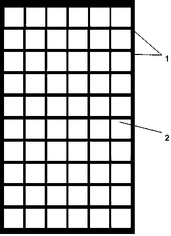
[0041] (1) Use the polyvinylidene fluoride casting solution containing titanium dioxide to coat the inner layer of the double-sided coated transparent substrate with a white grid structure; the coating method is screen printing or roller coating. The white grid structure is the area structure corresponding to the cell gap and frame when the photovoltaic module is packaged, and the width of the grid structure is designed according to the customer's module packaging requirements.
[0042] (2) Pre-evaporate the substrate coated with the white grid structure in the air; then the substrate treated in step (1) is precipitated and solidified by the phase inversion method; the phase inversion method is specifically: the step (1) The treated substrate is quickly immersed in a coagulation solution for 0.1-10 minutes; the coagulation solution is water or a mixed solution of water and an organ...
Embodiment 1
[0056] The inner layer of the double-sided coated transparent substrate is coated with white polyvinylidene fluoride casting liquid by screen printing, forming a cross at right angles such as figure 1 As shown, the formed transparent grid backplane structure is as follows image 3 As shown, the casting solution consists of 20 parts of polyvinylidene fluoride powder dissolved in 100 parts of N,N-dimethylformamide solvent under stirring at 60 ° C, and then adding 2 parts of Disperbyk 160 dispersant and 40 parts of The titanium dioxide is stirred and dispersed evenly; then it is precipitated and solidified in a water coagulation bath, and then processed in a 100°C drying tunnel for 3 minutes to obtain a 15μm white grid structure. A 275 μm thick PET film is selected as the transparent substrate, the thickness of the inner layer of the transparent substrate is 10 μm, and the thickness of the outer layer is 18 μm.
Embodiment 2
[0058] Roll coating white polyvinylidene fluoride casting solution on the inner layer of double-sided coated transparent substrate, forming a cross at right angles such as figure 1 As shown, the formed transparent grid backplane structure is as follows image 3 As shown, the casting solution is obtained by dissolving 30 parts of polyvinylidene fluoride powder in 100 parts of acetone solvent under stirring at 35°C, and then adding 1 part of Disperbyk 161 dispersant and 30 parts of titanium dioxide, stirring and dispersing evenly; Then precipitate and solidify in a coagulation bath of water / dipropylene glycol methyl ether=10 / 1, and then pass through a drying tunnel at 115°C for 3 minutes to obtain a white grid structure of 25 μm. A 250 μm thick PET film is selected as the transparent substrate, the thickness of the inner layer of the transparent substrate is 14 μm, and the thickness of the outer layer is 16 μm.
PUM
| Property | Measurement | Unit |
|---|---|---|
| thickness | aaaaa | aaaaa |
| thickness | aaaaa | aaaaa |
| thickness | aaaaa | aaaaa |
Abstract
Description
Claims
Application Information
 - R&D
- Intellectual Property
- Life Sciences
- Materials
- Tech Scout
- Unparalleled Data Quality
- Higher Quality Content
- 60% Fewer Hallucinations
Browse by: Latest US Patents, China's latest patents, Technical Efficacy Thesaurus, Application Domain, Technology Topic, Popular Technical Reports.
© 2025 PatSnap. All rights reserved.Legal|Privacy policy|Modern Slavery Act Transparency Statement|Sitemap|About US| Contact US: help@patsnap.com


