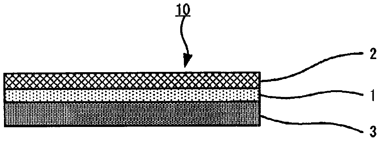
Method for producing electrode for solid-state batteries
A solid battery and manufacturing method technology, applied in the direction of electrode manufacturing, battery electrode, electrolyte battery manufacturing, etc., can solve the problems of battery temperature rise, battery adverse effects, etc., and achieve the effect of reducing electronic resistance
- Summary
- Abstract
- Description
- Claims
- Application Information
AI Technical Summary
Problems solved by technology
Method used
Image
Examples
no. 1 approach
[0080] Such as figure 2 As shown, the first embodiment of the manufacturing method of the present disclosure has at least two pressing processes: pressing process A1 of pressing the current collector formed with the PTC resistor layer; and pressing the electrode active material having at least the electrode active material layer Pressing process B in which the component is pressed.
[0081] 2-1. Process of forming PTC resistor layer
[0082] In the step of forming the PTC resistor layer of the first embodiment, the slurry containing the conductive material and the polymer is coated on at least one surface of the current collector and then dried to form the PTC resistor layer.
[0083] (1) Slurry
[0084] The paste contains conductive material and polymer.
[0085] The method of drying the slurry after coating the current collector to form the PTC resistor layer is not particularly limited, and generally, the conductive material and the polymer are dispersed in a non-aqueou...
no. 2 approach
[0127] Such as image 3 As shown, the second embodiment of the manufacturing method of the present disclosure has at least two pressing processes: the pressing process B of pressing the electrode active material member having at least the electrode active material layer 3 with a maximum pressure of b; and A pressing step A2 of pressing the electrode precursor having at least the current collector 2 , the electrode active material layer 3 and the PTC resistor layer 1 with a maximum pressure of a2 .
[0128] The first embodiment and the second embodiment are common in the following aspects: having at least two pressing processes; having the pressing process B of pressing an electrode active material member having at least an electrode active material layer; and The aspect in which the maximum pressure b1 applied to the electrode active material layer is greater than the maximum pressure applied to the PTC resistor body layer (a1 and a2).
[0129] On the other hand, in the step ...
Embodiment 1
[0153] (1-1) Step of forming PTC resistor layer
[0154] Furnace black (manufactured by Tokai Carbon Co., Ltd.) with an average primary particle size of 66 nm as a conductive material, alumina (particle size D90: 6 μm) as an insulating inorganic substance, and PVDF (Kureha Co., Ltd.) as a polymer were prepared. Made KF Polymer L #9130). These were mixed with N-methylpyrrolidone as a solvent so as to have a volume ratio of furnace black:PVDF:alumina=10:30:60 to prepare a slurry. Thereafter, the slurry was coated on an aluminum foil having a thickness of 15 μm, and dried in a stationary drying oven at 100° C. for 1 hour to form a PTC resistor layer.
[0155] (1-2) Pressing process A1
[0156] The current collector on which the PTC resistor layer was formed was rolled under conditions of a pressing pressure a1 of 5.6 kN / cm (converted value 199 MPa) and room temperature to obtain a PTC resistor layer-current collector laminate.
[0157] (1-3) Pressing process B, etc.
[0158] Li...
PUM
| Property | Measurement | Unit |
|---|---|---|
| thickness | aaaaa | aaaaa |
Abstract
Description
Claims
Application Information
 - R&D
- Intellectual Property
- Life Sciences
- Materials
- Tech Scout
- Unparalleled Data Quality
- Higher Quality Content
- 60% Fewer Hallucinations
Browse by: Latest US Patents, China's latest patents, Technical Efficacy Thesaurus, Application Domain, Technology Topic, Popular Technical Reports.
© 2025 PatSnap. All rights reserved.Legal|Privacy policy|Modern Slavery Act Transparency Statement|Sitemap|About US| Contact US: help@patsnap.com


