Method of manufacturing package and method of manufacturing light emitting device
A manufacturing method and a technology of a light-emitting device, which are applied in the direction of electric solid-state devices, semiconductor devices, electrical components, etc., can solve problems such as reduced visual recognition, and achieve the effect of reducing manufacturing costs
- Summary
- Abstract
- Description
- Claims
- Application Information
AI Technical Summary
Problems solved by technology
Method used
Image
Examples
no. 1 approach
[0064] [Manufacturing method of light-emitting device]
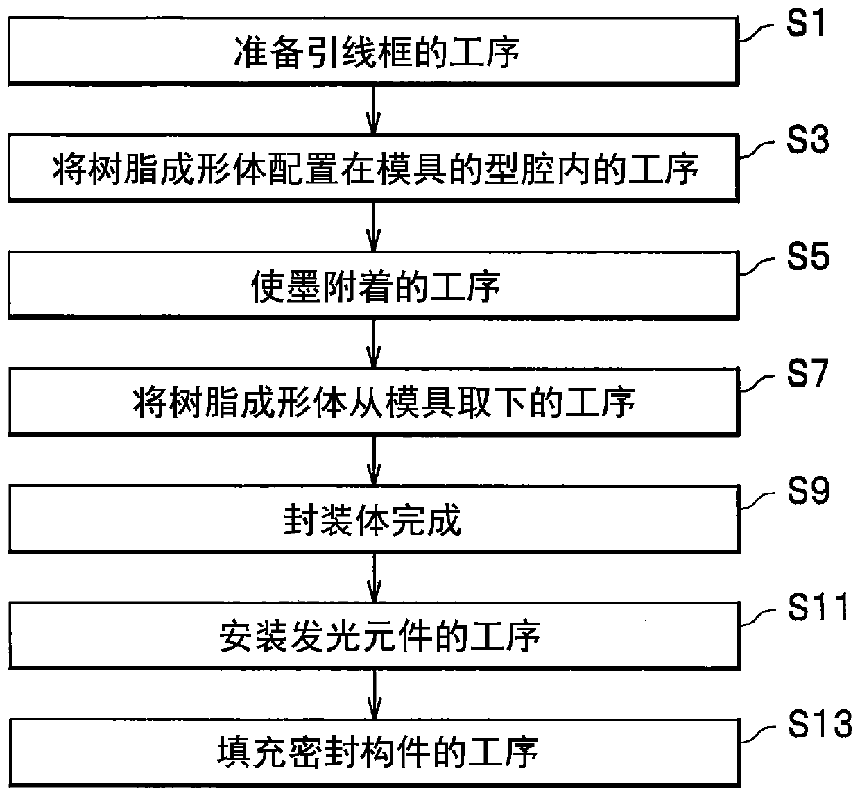
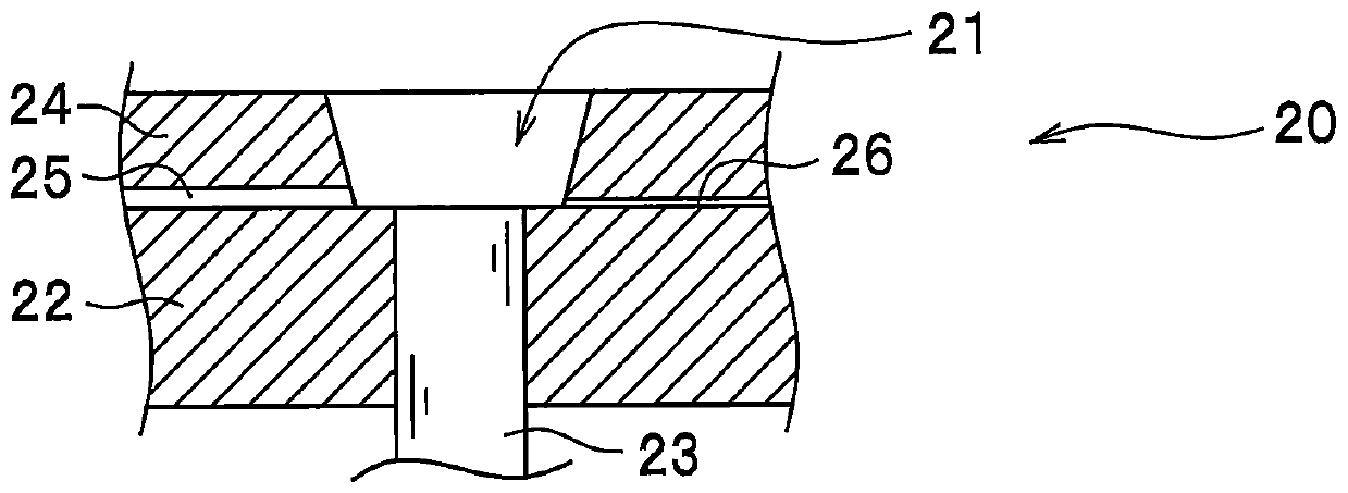
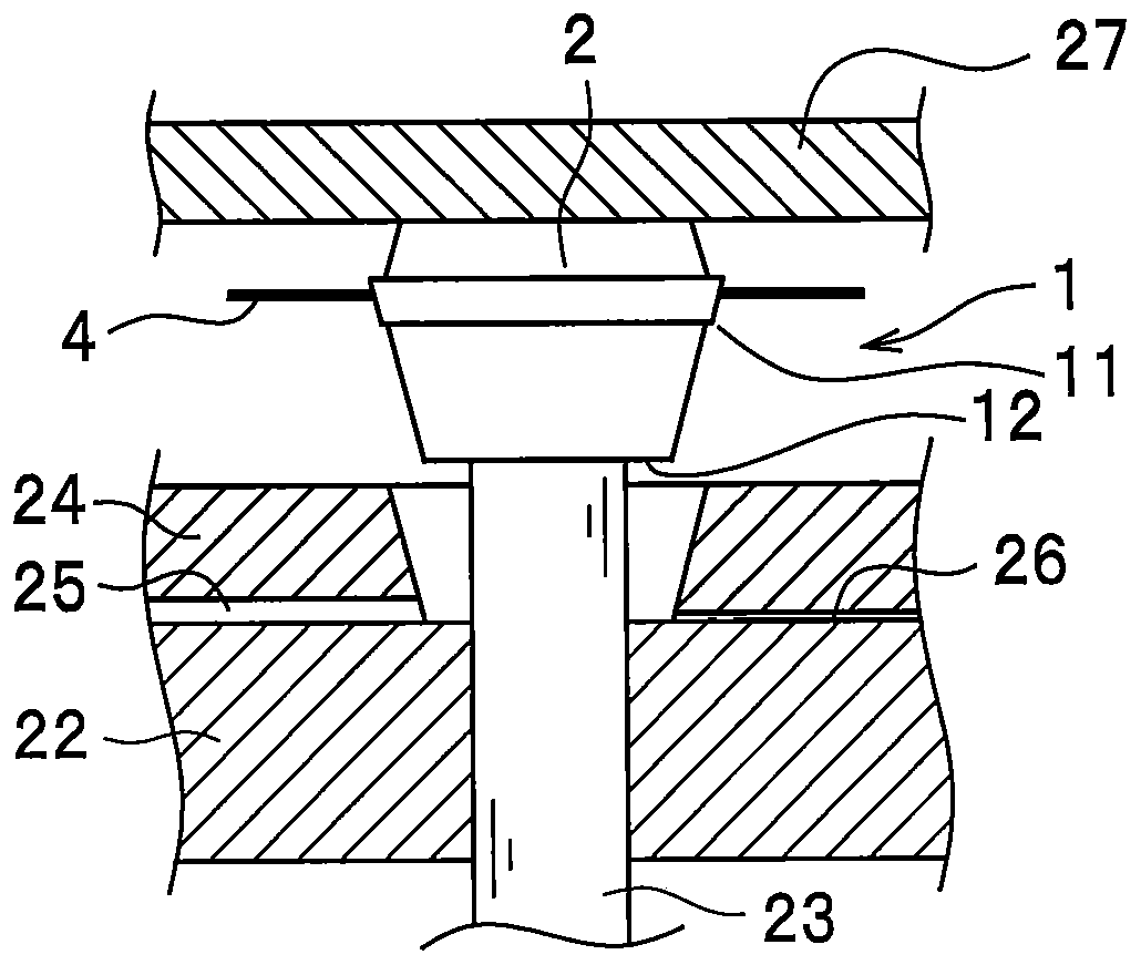
[0065] refer to figure 1 A method of manufacturing a light emitting device will be described. In addition, refer to Figure 2A ~ Figure 2F A method of manufacturing the package will be described. It should be noted that, for the convenience of explanation, in Figure 2A ~ Figure 2F , Figure 8A ~ Figure 8G and Figure 10 , a partial sectional view of the mold 20 and a side view of the ejector pin 23 and the resin molded body 2 are schematically shown. In addition, colorless means that the surface of the resin molded body is white, and small dots mean that a part of the surface of the resin molded body is black.
[0066] The method of manufacturing a light emitting device includes steps S1 to S7 of manufacturing a package, step S11 of mounting a light emitting element in a recess formed in the package, and step S13 of filling the recess with a sealing member so as to cover the light emitting element.
[0067] The m...
no. 2 approach
[0120] [Manufacturing method of light-emitting device]
[0121] Next, a method of manufacturing the light emitting device of the second embodiment will be described. Hereinafter, the same reference numerals are assigned to the same steps as those in the first embodiment, and description thereof will be omitted. In the manufacturing method of the light-emitting device in this embodiment, the steps S11 and S13 performed after the package is completed are the same as the manufacturing steps in the aforementioned first embodiment, and thus description thereof is omitted.
[0122] [Manufacturing method of package]
[0123] refer to Figure 8A ~ Figure 8G A method of manufacturing the package will be described.
[0124] The manufacturing method of the package of this embodiment includes: step S1, in this step, prepare the lead frame 1 provided with the lead 4 and the resin molded body 2, wherein the resin molded body 2 is molded integrally with the lead 4 and has on the upper sur...
no. 3 approach
[0137] [Manufacturing method of light-emitting device]
[0138] Next, a method of manufacturing the light emitting device of the third embodiment will be described. Hereinafter, the same reference numerals are assigned to the same steps as those in the second embodiment, and description thereof will be omitted. In the manufacturing method of the light-emitting device in this embodiment, the steps S11 and S13 performed after the package is completed are the same as the manufacturing steps in the aforementioned first embodiment, and thus description thereof is omitted.
[0139] [Manufacturing method of package]
[0140] refer to Figure 8A ~ Figure 8G , Figure 9 and Figure 10 A method of manufacturing the package will be described.
[0141] In the manufacturing method of the package of the present embodiment, the step of adhering the ink 5 includes a step 6 in which, after the resin molded body 2 is placed in the cavity 21 filled with the ink 5 , it is applied to the cavi...
PUM
 Abstract
Description
Claims
Application Information
 - R&D
- Intellectual Property
- Life Sciences
- Materials
- Tech Scout
- Unparalleled Data Quality
- Higher Quality Content
- 60% Fewer Hallucinations
Browse by: Latest US Patents, China's latest patents, Technical Efficacy Thesaurus, Application Domain, Technology Topic, Popular Technical Reports.
© 2025 PatSnap. All rights reserved.Legal|Privacy policy|Modern Slavery Act Transparency Statement|Sitemap|About US| Contact US: help@patsnap.com


