Light guide plate, manufacturing method thereof, surface light source device, and transmissive image display device
A manufacturing method and a technology for a light guide plate, which are applied in the field of light guide plates, and can solve the problems of a large difference in light and shade between a printing area and a non-printing area, and uneven grayscale of smoke haze.
- Summary
- Abstract
- Description
- Claims
- Application Information
AI Technical Summary
Problems solved by technology
Method used
Image
Examples
Embodiment 1)
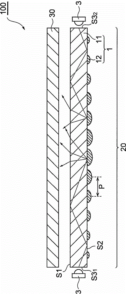
[0152] A PMMA resin sheet of 923 mm×540 mm was prepared as a translucent resin sheet, and a light guide plate was produced using an ultraviolet curable inkjet ink containing calcium carbonate as a pigment.
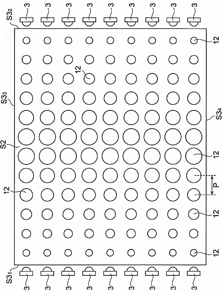
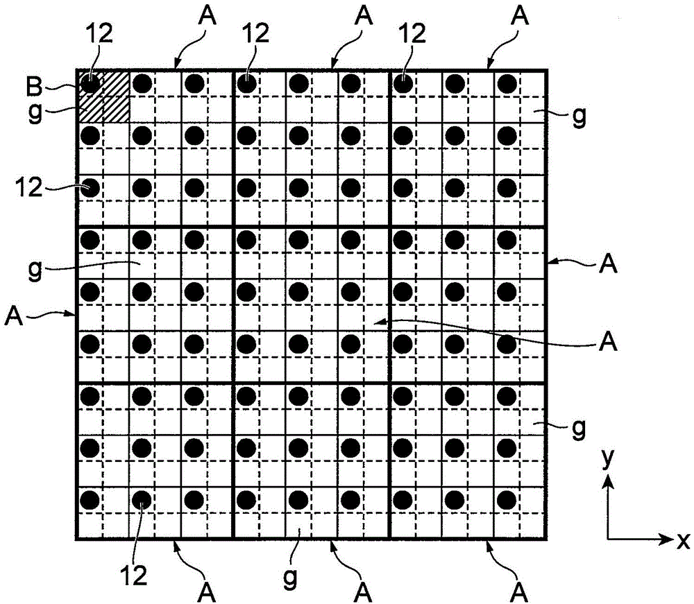
[0153] Specifically, according to Figure 5 As shown in the flowchart, the light distribution pattern is designed. In the coverage ratio setting step S11 , the back surface S2 was divided into a plurality of dummy regions A having a 507 μm square, and the coverage ratio of each dummy region A was set to 3.4%. Then, in the grid setting step S12 , 6×6 dummy grids g serving as printing targets of the light reflection dots 12 are set per dummy area A. FIG. In this process, 36 virtual grids g are regularly arranged two-dimensionally. In the virtual area A, the number ( L1 ) of virtual grids g in the first direction x is six, and in the virtual area A, the number ( L2 ) of virtual grids g in the second direction y is also six. Then, in the light reflection point condition set...
Embodiment 2~5)
[0159] The light guide plates of Examples 2 to 5 were obtained in the same manner as in Example 1 except that the arrangement of the light reflection points 12 in the dummy area A was changed.
[0160] Figure 8 (a)~ Figure 8 (d) is a drawing which shows the arrangement|positioning of the light reflection point 12 in the virtual area A in Examples 2-5, respectively. Differences between Embodiments 2 to 5 from Embodiment 1 will be described using the concept of the small area B. FIG. exist Figure 8 (a)~ Figure 8 (d), in order to represent the size of the small area B, with Figure 4 In the same case, a small area B is marked with oblique lines. In the other drawings, a small area B is also marked with oblique lines.
[0161] In Embodiment 2, the configuration of the light reflection points 12 in the small area B is as follows Figure 8 It is changed as shown in (a). In Example 2, the light reflection points 12 are arranged for all the small areas B in the virtual are...
Embodiment 6)
[0168] In Example 6, the coverage rate was changed to 1.9%, and the number (n) of light reflection points 12 in the virtual area A was changed to five. As the number (n) of light reflection points 12 changes, the configuration of light reflection points 12 in the virtual area A is as follows: Figure 9 It is changed as shown in (a). Figure 9 (a) is a figure which shows the arrangement|positioning of the light reflection point 12 in the virtual area A in Example 6. FIG. In Example 6, the number (n) of light reflection points 12 in the virtual area A is 5, and L1 and L2 are 6 as in Example 1, so N1e min with N2e min The combination of is (2, 3) or (3, 2). In Example 6, it is assumed that N1e min = 2, N2e min =3. Therefore, when the concept of small area B is introduced in the same manner as in Example 1, the number (M1) of virtual grids g in the first direction x constituting the small area B in Example 6 is three, and the number of virtual grids g in the second direction...
PUM
| Property | Measurement | Unit |
|---|---|---|
| thickness | aaaaa | aaaaa |
| viscosity | aaaaa | aaaaa |
Abstract
Description
Claims
Application Information
 - R&D
- Intellectual Property
- Life Sciences
- Materials
- Tech Scout
- Unparalleled Data Quality
- Higher Quality Content
- 60% Fewer Hallucinations
Browse by: Latest US Patents, China's latest patents, Technical Efficacy Thesaurus, Application Domain, Technology Topic, Popular Technical Reports.
© 2025 PatSnap. All rights reserved.Legal|Privacy policy|Modern Slavery Act Transparency Statement|Sitemap|About US| Contact US: help@patsnap.com


