Light guide plate and method of manufacturing light guide plate, surface light source apparatus and transmission type image display apparatus
A manufacturing method and technology of light guide plates, applied in the field of light guide plates, can solve problems such as uneven gray scale of smog, large difference between light and shade in printing area and non-printing area, etc.
- Summary
- Abstract
- Description
- Claims
- Application Information
AI Technical Summary
Problems solved by technology
Method used
Image
Examples
Embodiment 1)
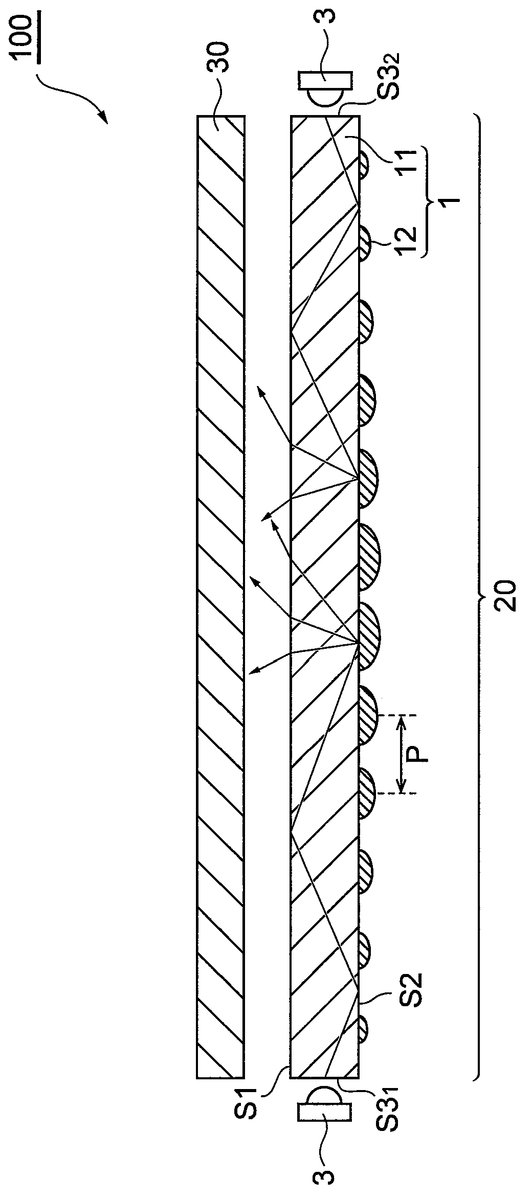
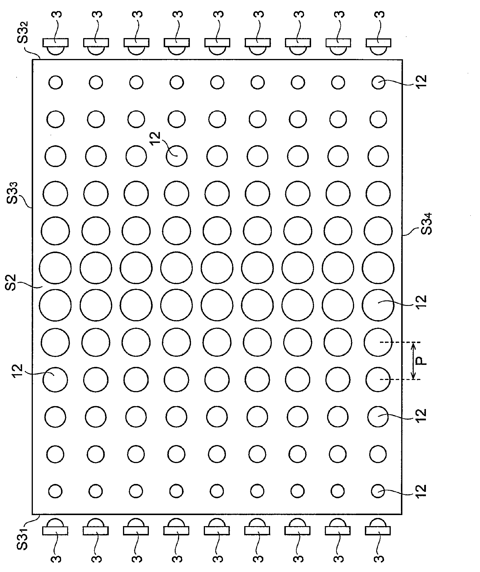
[0152] A PMMA resin sheet of 923 mm×540 mm was prepared as a translucent resin sheet, and a light guide plate was produced using an ultraviolet curable inkjet ink containing calcium carbonate as a pigment.
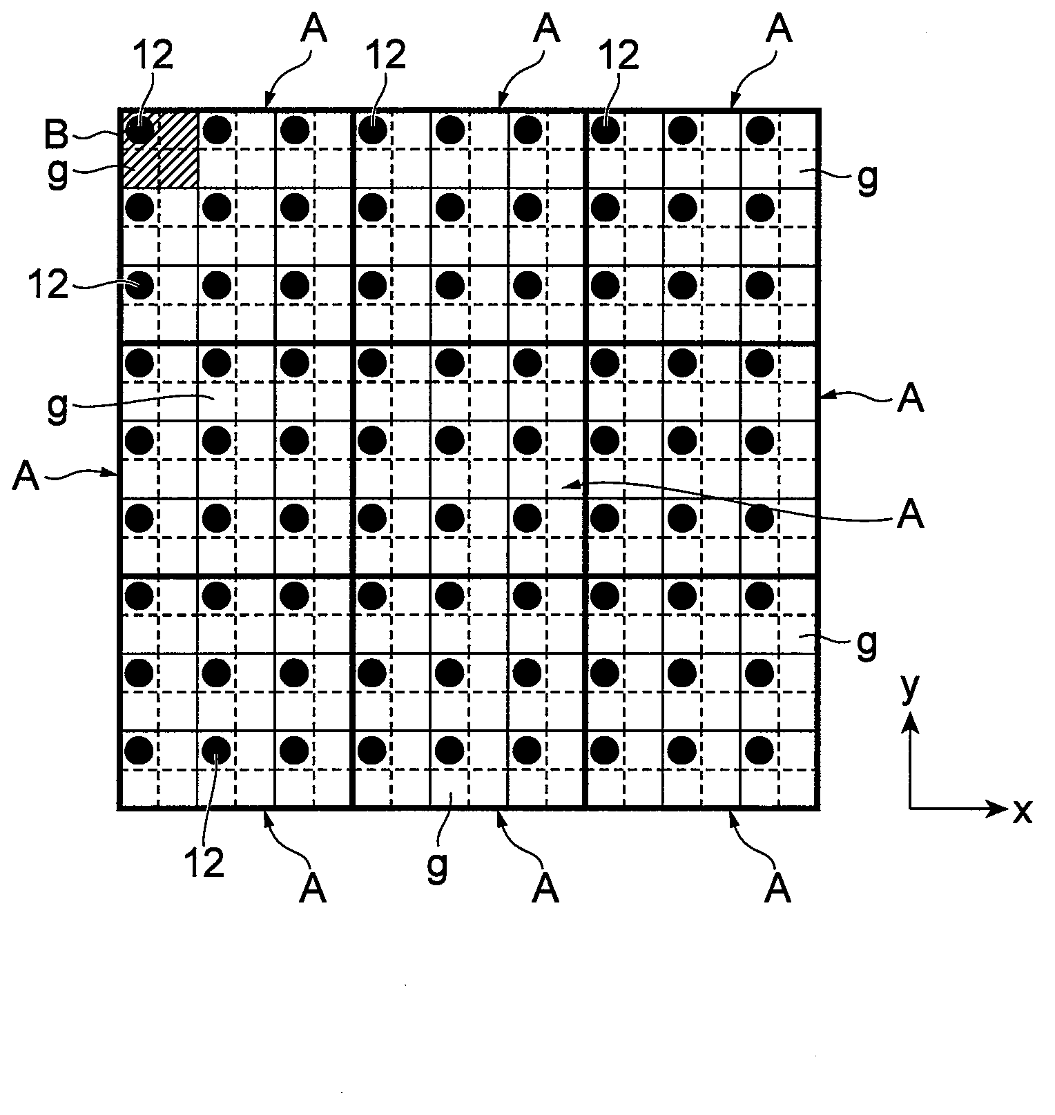
[0153] Specifically, according to Figure 5 As shown in the flowchart, the light distribution pattern is designed. In the coverage ratio setting step S11 , the back surface S2 was divided into a plurality of dummy regions A having a 507 μm square, and the coverage ratio of each dummy region A was set to 3.4%. Then, in the grid setting step S12 , 6×6 dummy grids g serving as printing targets of the light reflection dots 12 are set per dummy area A. FIG. In this process, 36 virtual grids g are regularly arranged two-dimensionally. In the virtual area A, the number ( L1 ) of virtual grids g in the first direction x is six, and in the virtual area A, the number ( L2 ) of virtual grids g in the second direction y is also six. Then, in the light reflection point condition set...
Embodiment 2~5)
[0159] The light guide plates of Examples 2 to 5 were obtained in the same manner as in Example 1 except that the arrangement of the light reflection points 12 in the dummy area A was changed.
[0160] Figure 8 (a)~ Figure 8 (d) is a drawing which shows the arrangement|positioning of the light reflection point 12 in the virtual area A in Examples 2-5, respectively. Differences between Embodiments 2 to 5 from Embodiment 1 will be described using the concept of the small area B. FIG. exist Figure 8 (a)~ Figure 8 (d), in order to represent the size of the small area B, with Figure 4 In the same case, a small area B is marked with oblique lines. In the other drawings, a small area B is also marked with oblique lines.
[0161] In Embodiment 2, the configuration of the light reflection points 12 in the small area B is as follows Figure 8 It is changed as shown in (a). In Example 2, the light reflection points 12 are arranged for all the small areas B in the virtual are...
Embodiment 6)
[0168] In Example 6, the coverage rate was changed to 1.9%, and the number (n) of light reflection points 12 in the virtual area A was changed to five. As the number (n) of light reflection points 12 changes, the configuration of light reflection points 12 in the virtual area A is as follows: Figure 9 It is changed as shown in (a). Figure 9 (a) is a figure which shows the arrangement|positioning of the light reflection point 12 in the virtual area A in Example 6. FIG. In Example 6, the number (n) of light reflection points 12 in the virtual area A is 5, and L1 and L2 are 6 as in Example 1, so N1e min with N2e min The combination of is (2, 3) or (3, 2). In Example 6, it is assumed that N1e min = 2, N2e min =3. Therefore, when the concept of small area B is introduced in the same manner as in Example 1, the number (M1) of virtual grids g in the first direction x constituting the small area B in Example 6 is three, and the number of virtual grids g in the second direction...
PUM
| Property | Measurement | Unit |
|---|---|---|
| thickness | aaaaa | aaaaa |
| viscosity | aaaaa | aaaaa |
Abstract
Description
Claims
Application Information
 - R&D
- Intellectual Property
- Life Sciences
- Materials
- Tech Scout
- Unparalleled Data Quality
- Higher Quality Content
- 60% Fewer Hallucinations
Browse by: Latest US Patents, China's latest patents, Technical Efficacy Thesaurus, Application Domain, Technology Topic, Popular Technical Reports.
© 2025 PatSnap. All rights reserved.Legal|Privacy policy|Modern Slavery Act Transparency Statement|Sitemap|About US| Contact US: help@patsnap.com


