A kind of organic optoelectronic device packaging film and preparation method thereof

A technology for optoelectronic devices and encapsulation films, which is applied in the field of organic optoelectronic device encapsulation films and its preparation, can solve problems such as inability to effectively block water and oxygen, large surface roughness, and poor compactness, and achieve improved visible light transmittance and reduced defects The effect of increasing the number and improving the density

Active Publication Date: 2020-12-29
JILIN UNIV
View PDF6 Cites 0 Cited by
  • Summary
  • Abstract
  • Description
  • Claims
  • Application Information

AI Technical Summary

Problems solved by technology

[0003] The purpose of the present invention is to provide a packaging film for organic photoelectric devices and its preparation method, which is used to solve the problems of large surface roughness and poor compactness in packaging films grown by chemical vapor deposition and physical vapor deposition in organic photoelectric devices. There may even be defects such as pinhole cracks, which cannot effectively block water and oxygen.

Method used


Image

  • A kind of organic optoelectronic device packaging film and preparation method thereof
  • A kind of organic optoelectronic device packaging film and preparation method thereof
  • A kind of organic optoelectronic device packaging film and preparation method thereof

Examples


Embodiment 1

[0032] An embodiment of the present invention provides a method for manufacturing an encapsulation film, including:

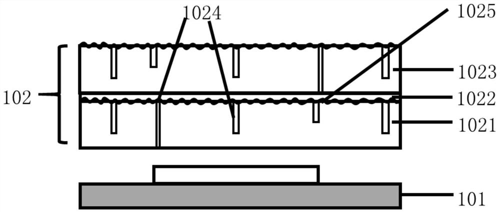
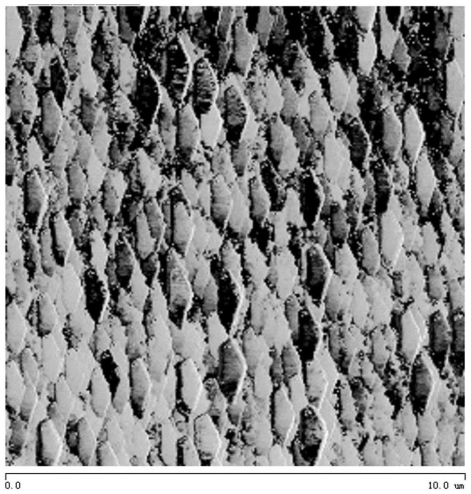
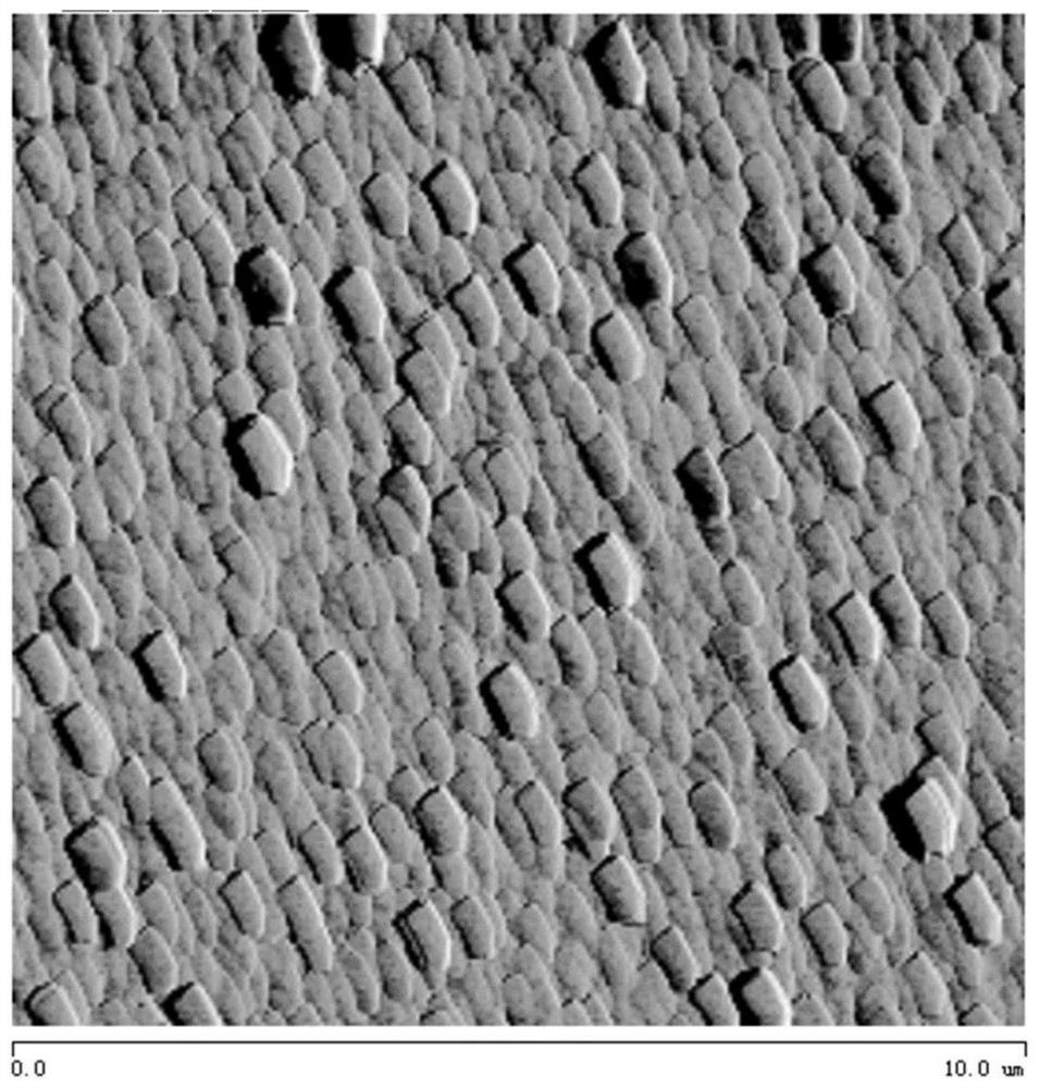
[0033] (1) The structure to be packaged is ITO / MoO by inductively coupled plasma enhanced chemical vapor deposition process x (2nm) / m-MTDATA(30nm) / NPB(20nm) / Alq(50nm) / LiF(0.5nm) / Al(100nm) organic optoelectronic devices grow the first encapsulation layer: inductively coupled plasma before passing reactive gas Volume-enhanced chemical vapor deposition equipment (low temperature ICP-PECVD system, model: ICP-PECVD-150) the vacuum in the chamber is 3 × 10 -5 Torr. With hexamethyldisiloxane (HMDSO) as the reaction precursor, the flow rate is 0.08g / min; with argon (Ar) as the auxiliary reaction gas, the flow rate is 30sccm, with O 2 For the reaction gas, the flow rate is 158 sccm. During the process, the vacuum degree is 273mTorr, the reaction temperature is 77°C, and the radio frequency power is 100W. The reaction produces silicon oxide (SiO x ) is the first enc...


PUM

PropertyMeasurementUnit
thicknessaaaaaaaaaa
thicknessaaaaaaaaaa
mean roughnessaaaaaaaaaa

Abstract

An organic photoelectric device encapsulation film and a preparation method thereof belong to the technical field of film encapsulation. It is to grow the first encapsulation layer on the organic optoelectronic device to be encapsulated, and then grow a thin metal single substance layer on the first encapsulation layer and then perform chemical treatment in situ to form the second encapsulation layer, and finally pass the first encapsulation layer and The alternate growth of the second encapsulation layer completes the preparation of the organic photoelectric device encapsulation film. The thin metal layer increases the surface roughness of the first encapsulation layer, and then the reactive gas plasma treatment enables the metal atoms in the thin metal layer to obtain high enough energy to be redistributed on the surface of the first encapsulation layer, while the original The metal compound is generated by bit reaction, and as the second encapsulation layer, it fills the defects on the surface of the first encapsulation layer, improves the water and oxygen barrier ability, increases the visible light transmittance, and improves the encapsulation effect. Experiments show that after 2.5 cycles, the water vapor transmission rate of the film can reach 10 ‑5 g·m ‑2 ·day ‑1 order of magnitude.

Description

technical field [0001] The invention belongs to the technical field of film encapsulation, and in particular relates to an organic photoelectric device encapsulation film and a preparation method thereof. Background technique [0002] Organic optoelectronic devices, such as organic light-emitting diodes, organic solar cells, organic field-effect transistors, etc., are widely used in display, energy, medical and other fields due to their advantages of flexibility, large-area integration, and all-solid-state. Because its organic functional layer is particularly sensitive to water vapor and oxygen in the air, it is easily corroded by water and oxygen, which will cause the performance of organic photoelectric devices to degrade or even fail. Therefore, organic photoelectric devices need to be packaged to ensure the performance and service life of the device. At present, the commonly used packaging method for organic optoelectronic devices is thin-film packaging with organic-inor...

Claims


Application Information

Patent Timeline
Patent Type & Authority Patents(China)
IPC IPC(8): H01L51/50H01L51/52H01L51/56
CPCH10K50/00H10K50/84H10K71/00
Inventor 赵毅秦后运刘畅刘一鸣魏松彭翀
Owner JILIN UNIV
Why Eureka
Try Eureka