Composite SERS substrate and preparation method and application thereof
A technology of substrate and bottom layer, applied in the field of composite SERS substrate and its preparation, can solve the problems of low detection resolution of chemical pesticide molecules, weak intensity of ordinary Raman signal, and difficulty in identifying molecular information, and achieves good consistency and detection limit. Low, easy-to-use effects
- Summary
- Abstract
- Description
- Claims
- Application Information
AI Technical Summary
Problems solved by technology
Method used
Image
Examples
preparation example Construction
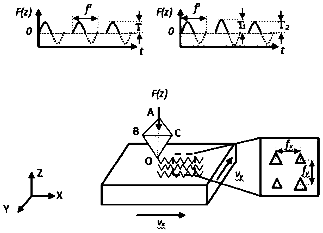
[0026] The invention provides a kind of preparation method of composite SERS substrate, comprises the following steps:
[0027] The micro-nano structure is prepared on the surface layer of the two-dimensional material by using a nano-indentation instrument to obtain a composite SERS substrate;
[0028] The two-dimensional material includes a metal bottom layer and a graphene surface layer arranged in layers.
[0029] In the present invention, the thickness of the metal bottom layer is preferably 5-10 μm, more preferably 6 μm, 7 μm, 8 μm or 9 μm; the thickness of the graphene surface layer is preferably 1-3 nm, more preferably 1.5 nm, 2 nm or 2.5 nm. nm. In the present invention, the metal in the metal bottom layer preferably includes gold, silver or copper, more preferably copper. In the present invention, the two-dimensional material is preferably a commercially available product well known to those skilled in the art. In the present invention, the graphene surface layer o...
Embodiment 1
[0045] A nano-indentation instrument is used to prepare a micro-nano structure on the graphene surface layer of a two-dimensional material to obtain a composite SERS substrate; the two-dimensional material includes a copper bottom layer and a graphene surface layer; the working parameters of the nano-indentation instrument are: use a diamond triangular pyramid probe needle (the angle between the three surfaces is 120°, the arc radius is x is 5μm / s, the loading rate v of the workbench in the Y direction y is 5μm / s.
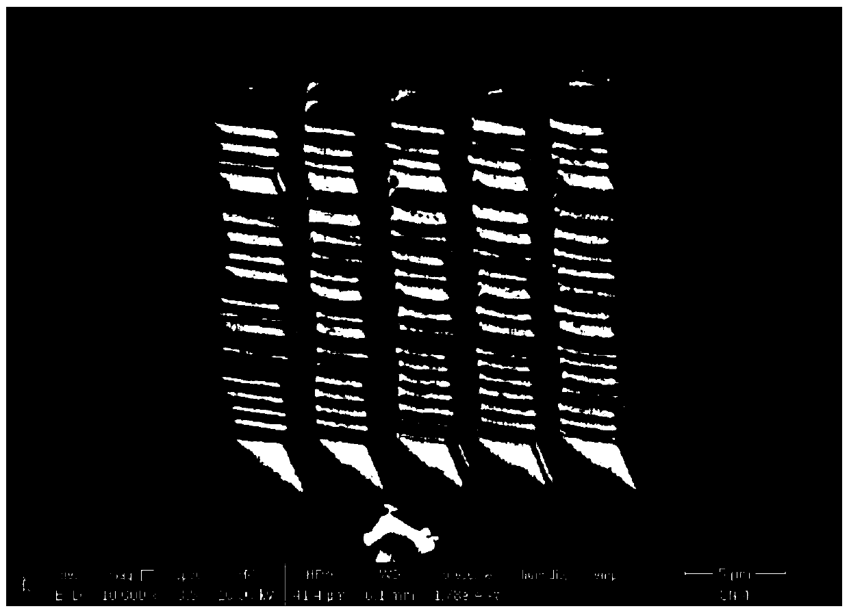
[0046] The area of the lattice micro-nano structure on the surface of the composite SERS substrate is 20×20 μm 2 , its SEM image is shown in figure 2 shown by figure 2 It can be seen that when the loading rate of the table in the X and Y directions is 5 μm / s, two adjacent indentations are connected, and the depth of a single indentation is 1.2 μm.
Embodiment 2
[0048] Composite SERS substrate is prepared according to the method of Example 1, and the difference with Example 1 is that v y is 1 μm / s.
[0049] The area of the lattice micro-nano structure on the surface of the composite SERS substrate is 20×20 μm 2 , its SEM image is shown in image 3 shown by image 3 It can be seen that when the loading rate of the table in the X and Y directions is less than 5 μm / s, two adjacent indentations overlap, and the depth of a single indentation is 0.4 μm.
PUM
| Property | Measurement | Unit |
|---|---|---|
| Depth | aaaaa | aaaaa |
| Thickness | aaaaa | aaaaa |
| Thickness | aaaaa | aaaaa |
Abstract
Description
Claims
Application Information
 - R&D
- Intellectual Property
- Life Sciences
- Materials
- Tech Scout
- Unparalleled Data Quality
- Higher Quality Content
- 60% Fewer Hallucinations
Browse by: Latest US Patents, China's latest patents, Technical Efficacy Thesaurus, Application Domain, Technology Topic, Popular Technical Reports.
© 2025 PatSnap. All rights reserved.Legal|Privacy policy|Modern Slavery Act Transparency Statement|Sitemap|About US| Contact US: help@patsnap.com


