Optically controlled memristor and preparation method thereof
A technology of memristor and spin-coating method, which is applied in the field of memory, can solve the problems of single working mode and high energy consumption of memristor, and achieve the effects of high light absorption coefficient, high carrier mobility, and reduced operating voltage
- Summary
- Abstract
- Description
- Claims
- Application Information
AI Technical Summary
Problems solved by technology
Method used
Image

Examples
preparation example Construction
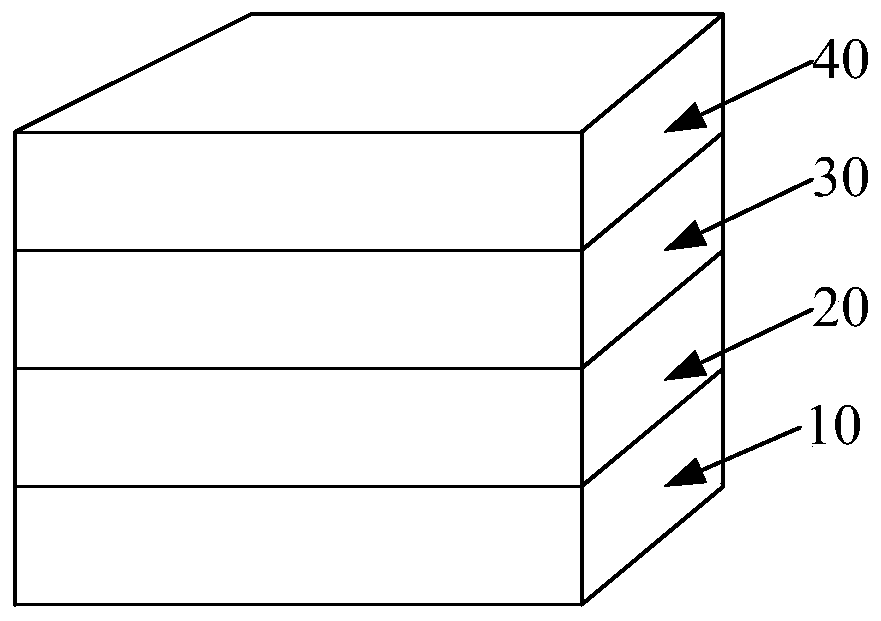
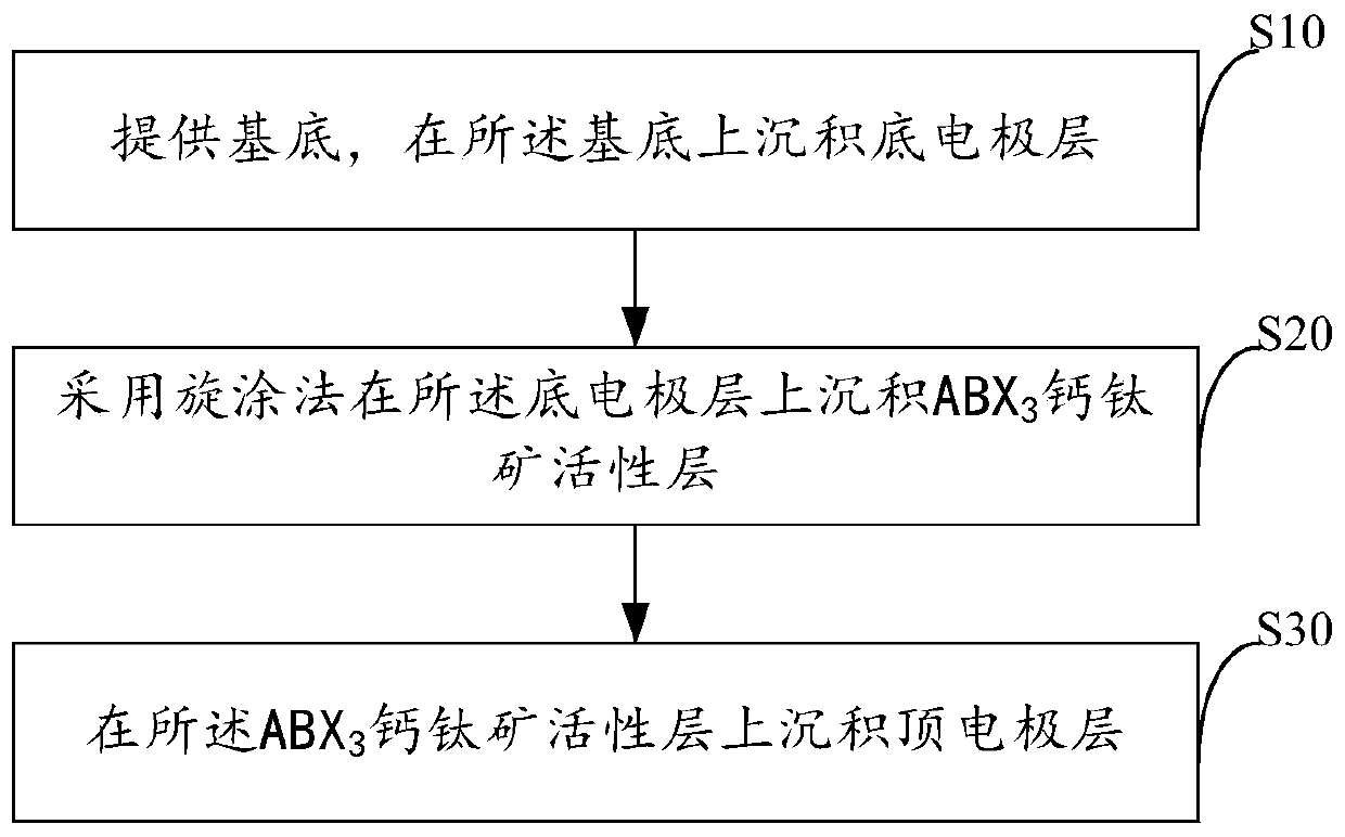
[0033] further, such as image 3 As shown, the present invention also provides a method for preparing an optically controlled memristor, the method comprising the steps of:
[0034] S10, providing a substrate, and depositing a bottom electrode layer on the substrate;
[0035] As an example, glass can be used as the substrate, and the surface of the substrate material is cleaned for use; indium tin oxide (ITO) is used as the bottom electrode material, and a certain thickness of ITO is sputtered on the glass substrate by magnetron sputtering as the bottom of the device. electrode.
[0036] S20, depositing ABX on the bottom electrode layer by spin coating 3 Perovskite active layer;
[0037] Specifically, first prepare ABX 3 The perovskite precursor is now based on methylammonium lead iodide (MAPbI 3 ) perovskite active layer preparation as an example to explain. Take DMSO, MAI and PbI with a molar mass ratio of 1:1:1, respectively 2, and dissolve the mixture in DMF solvent...
Embodiment 1
[0042] (1) Preparation of perovskite precursor solution:
[0043] Weigh DMSO, CsBr and PbBr with a molar mass ratio of 1:1:1, respectively 2 , and the mixture was dissolved in DMF solvent, stirred to make it evenly mixed and set aside.
[0044] (2) Preparation of optically controlled memristor:
[0045] Using PET as the substrate, 300nm AZO was sputtered on the PET substrate by magnetron sputtering as the bottom electrode of the device, and then CsPbBr was prepared by a one-step solution method 3 Perovskite active layer. CbBr 3 The preparation method of the perovskite active layer is as follows:
[0046] CsPbBr 3 Add the perovskite precursor solution dropwise on the PET substrate with the AZO layer, start the spin coater, accelerate the spin coater to 5000rpm in 5s, spin coat at 5000rpm for 40s, and drop in the Chlorobenzene was used as a reverse solvent to promote the crystallization of perovskite; the spin-coated sheet was pre-annealed on a hot stage at 65 degrees Cels...
Embodiment 2
[0048] (1) Preparation of perovskite precursor solution:
[0049] Weigh DMSO, CsI and PbI with a molar mass ratio of 1:1:1, respectively 2 , and the mixture was dissolved in DMF solvent, stirred to make it evenly mixed and set aside.
[0050] (2) Preparation of optically controlled memristor:
[0051] Using glass as the substrate, 300nm ITO was sputtered on the glass substrate by magnetron sputtering method as the bottom electrode of the device, and then CsPbI was prepared by a one-step solution method 3 Perovskite active layer. CaPbI 3 The preparation method of the perovskite active layer is as follows:
[0052] CsPbI 3 The perovskite precursor solution is added dropwise on the glass substrate with the ITO layer, start the spin coater, accelerate the spin coater to 4000rpm in 5s, spin coat at 4000rpm for 30s, and drop in the Chlorobenzene was used as a reverse solvent to promote the crystallization of perovskite; the spin-coated sheet was pre-annealed on a hot stage at ...
PUM
| Property | Measurement | Unit |
|---|---|---|
| thickness | aaaaa | aaaaa |
| thickness | aaaaa | aaaaa |
| thickness | aaaaa | aaaaa |
Abstract
Description
Claims
Application Information
 - Generate Ideas
- Intellectual Property
- Life Sciences
- Materials
- Tech Scout
- Unparalleled Data Quality
- Higher Quality Content
- 60% Fewer Hallucinations
Browse by: Latest US Patents, China's latest patents, Technical Efficacy Thesaurus, Application Domain, Technology Topic, Popular Technical Reports.
© 2025 PatSnap. All rights reserved.Legal|Privacy policy|Modern Slavery Act Transparency Statement|Sitemap|About US| Contact US: help@patsnap.com