A method for preparing silicon carbide single crystal based on controllable growth center
A technology of silicon carbide single crystal and silicon carbide seed is applied in the field of preparing silicon carbide single crystal based on a controllable growth center, which can solve the problems of increasing the probability of crystal cracking, reducing the yield of single crystal, and non-uniform polymorphism, and achieving Small internal stress, improved electrical uniformity, and small residual internal stress
- Summary
- Abstract
- Description
- Claims
- Application Information
AI Technical Summary
Problems solved by technology
Method used
Image


Examples
Embodiment 1
[0055] (1) Grinding and polishing a 4-inch silicon carbide seed crystal with a large diameter of 4° (diameter 105 mm) on both sides, so that the surface roughness is less than 0.3 nm and the flatness is 10 μm, and a silicon carbide seed crystal with a thickness of 500 μm is obtained. Then the surface is cleaned and packaged for use.
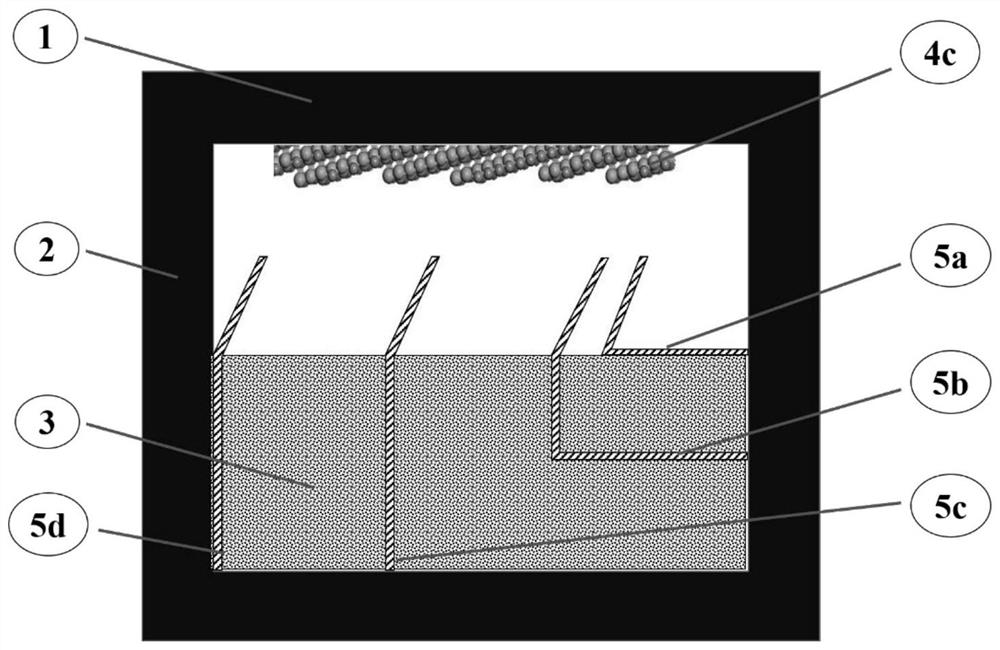
[0056] (2) Place a deflected growth component deflector in the powder and growth chamber: open four slots inside the graphite crucible tube, place four deflectors in the slots and fix them so that the deflectors The powder is divided into 3 regions with different volumes, and the part of the deflector located in the growth chamber is used to adjust the inclination angle of the component flow direction; the upper inclination angle of the deflector is 65 °, and the extension line of the deflector 5a is in line with the The edges of the large-diameter seed crystals just intersect, and the deflector not only plays the role of separating the silicon c...
Embodiment 2
[0063] (1) Grinding and polishing a 4-inch silicon carbide seed crystal with a large diameter of 5° (diameter 105 mm) on both sides, so that the surface roughness is less than 0.3 nm, and the flatness is 10 μm, and a silicon carbide seed crystal with a thickness of 500 μm is obtained. Then the surface is cleaned and packaged for use.
[0064] (2) Place a deflected growth component deflector in the powder and growth chamber: open four slots inside the graphite crucible tube, place four deflectors in the slots and fix them so that the deflectors The powder is divided into 3 different volume regions, and the part of the deflector located in the growth chamber is used to adjust the inclination angle of the component flow direction; the upper inclination angle of the deflector is 70 °, and the extension line of the deflector 5a is in line with the The edges of the large-diameter seed crystals just intersect, and the deflector not only plays the role of separating the silicon carbid...
Embodiment 3
[0070] (1) Grind and polish the 8-inch silicon carbide seed crystal with a large diameter of 8° on both sides, so that the surface roughness is less than 0.3nm, and the flatness is 10μm, and a silicon carbide seed crystal with a thickness of 500μm is obtained, and then the surface is cleaned. Clean and pack for use.
[0071] (2) Place a deflected growth component deflector in the powder and growth chamber: open four slots inside the graphite crucible tube, place four deflectors in the slots and fix them so that the deflectors The powder is divided into 3 regions with different volumes, and the part of the deflector located in the growth chamber is used to adjust the inclination angle of the component flow direction; the inclination angle of the upper part of the deflector is 75 °, and the extension line of the deflector 5a is in line with the The edges of the large-diameter seed crystals just intersect, and the deflector not only plays the role of separating the silicon carbid...
PUM
| Property | Measurement | Unit |
|---|---|---|
| surface roughness | aaaaa | aaaaa |
| thickness | aaaaa | aaaaa |
| surface roughness | aaaaa | aaaaa |
Abstract
Description
Claims
Application Information
 - R&D
- Intellectual Property
- Life Sciences
- Materials
- Tech Scout
- Unparalleled Data Quality
- Higher Quality Content
- 60% Fewer Hallucinations
Browse by: Latest US Patents, China's latest patents, Technical Efficacy Thesaurus, Application Domain, Technology Topic, Popular Technical Reports.
© 2025 PatSnap. All rights reserved.Legal|Privacy policy|Modern Slavery Act Transparency Statement|Sitemap|About US| Contact US: help@patsnap.com