A closed planar three-electrode spark switch and its preparation method
A spark switch, three-electrode technology, used in spark plugs, spark gaps, spark gap components, etc., can solve the problem of unstable self-breakdown performance and conduction performance of switches, the influence of circuits around the spark, and the performance of high overload resistance. It can achieve the effect of shortening the processing cycle, low price and strong ablation resistance.
- Summary
- Abstract
- Description
- Claims
- Application Information
AI Technical Summary
Problems solved by technology
Method used
Image
Examples
preparation example Construction
[0035] The preparation process of the closed planar three-electrode switch is as follows:
[0036] The process includes the following specific steps:
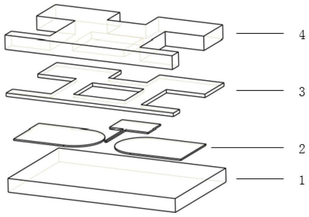
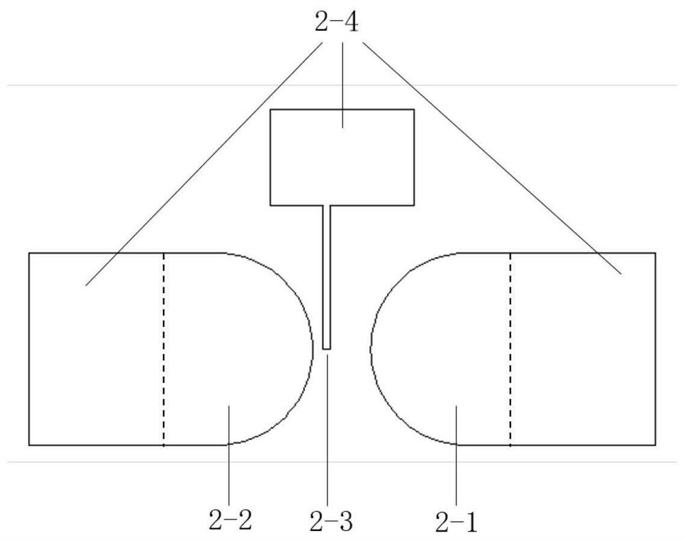
[0037] The first step is to clean the bottom PCB (1) board, and use the methods of exposure, development and etching to apply copper on the upper surface of the bottom PCB board 1 to obtain the circuit pattern corresponding to the switch, including the anode 2-1 of the switch , the cathode 2-2, the trigger electrode 2-3 and the pad 2-4 connected to it.
[0038] The second step is to perform chemical nickel-gold or tin spraying process treatment on the pads 2-4 on the circuit layer to ensure the solderability and flatness of the pads; the anode 2-1 and the cathode 2-2 on the circuit layer are Processes such as immersion gold or gold plating are performed on the trigger electrodes 2-3 to prevent the electrodes from being oxidized.
[0039] The fourth step is to use laser or mechanical cutting to open windows in the area corresp...
Embodiment 1
[0044]This implementation case designs a closed plane three-electrode spark switch based on printed circuit board technology. According to the printed circuit board technology, combined with its processing steps, the switch can be divided into four parts: the bottom PCB board 1, the circuit layer 2, the PP layer 3 and the top PCB board 4. The thickness of the bottom PCB board 1 is 1mm, and the material is FR-4, which is used as the carrier of the circuit layer in the whole switch. The circuit layer 2 directly etches the copper on the upper surface of the bottom PCB board 1 by the processes of printing oil, developing, etching, and film stripping to obtain the pattern corresponding to the switch. The thickness of the circuit layer is 35 μm. The circuit layer includes three electrodes of the planar three-electrode switch, namely the anode 2-1, the cathode 2-2, the trigger electrode 2-3 and the three pads 2-4 connected to it; the anode and the cathode are semicircular electrodes....
PUM
| Property | Measurement | Unit |
|---|---|---|
| thickness | aaaaa | aaaaa |
| thickness | aaaaa | aaaaa |
| thickness | aaaaa | aaaaa |
Abstract
Description
Claims
Application Information
 - R&D
- Intellectual Property
- Life Sciences
- Materials
- Tech Scout
- Unparalleled Data Quality
- Higher Quality Content
- 60% Fewer Hallucinations
Browse by: Latest US Patents, China's latest patents, Technical Efficacy Thesaurus, Application Domain, Technology Topic, Popular Technical Reports.
© 2025 PatSnap. All rights reserved.Legal|Privacy policy|Modern Slavery Act Transparency Statement|Sitemap|About US| Contact US: help@patsnap.com


