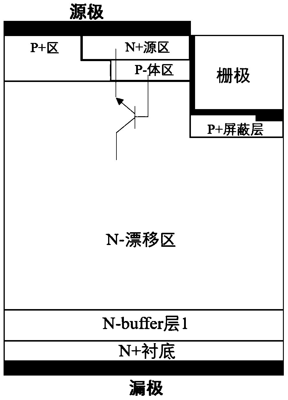
Half-cell structure of gate power MOSFET anti-single-particle-burnout device
An anti-single particle, power technology, applied in semiconductor devices, electrical components, circuits, etc., can solve the problem of not meeting the requirements of low power consumption of aerospace semiconductor devices, increasing the reverse leakage current density of the device, and the forward conduction current density of the device. It can improve the anti-SEB performance, reduce the peak value of the electric field and impact ionization, and improve the anti-SEB performance.
- Summary
- Abstract
- Description
- Claims
- Application Information
AI Technical Summary
Problems solved by technology
Method used
Image

Examples
Embodiment Construction
[0015] In order to make the objectives, technical solutions and advantages of the present invention clearer, the present invention will be described in detail below with reference to the accompanying drawings.
[0016] Since the deep trench electrode structure of the present invention is suitable for all power semiconductor devices containing parasitic BJT structures, the following simulation verification method is only used for figure 1 with figure 2 The two structures shown are compared and discussed:
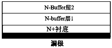
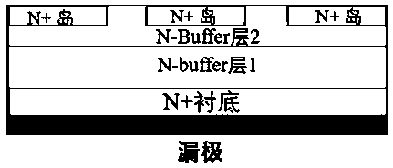
[0017] ①. Select 1200V gate power MOSFET device, the cell width is 8.4μm, the thickness is 14.5μm; the drift zone concentration is 4.0×10 15 cm -3 , The thickness of the gate oxide layer is 0.05μm;
[0018] ②. The linear energy transfer (LET) of incident ions is 0.1pC / μm, and the incident trajectory is at the edge of the channel (normal incidence and runs through the entire device); the charge density generated by incident ions is Gaussian distribution: the radius of the trajectory ...
PUM
 Abstract
Description
Claims
Application Information
 - R&D
- Intellectual Property
- Life Sciences
- Materials
- Tech Scout
- Unparalleled Data Quality
- Higher Quality Content
- 60% Fewer Hallucinations
Browse by: Latest US Patents, China's latest patents, Technical Efficacy Thesaurus, Application Domain, Technology Topic, Popular Technical Reports.
© 2025 PatSnap. All rights reserved.Legal|Privacy policy|Modern Slavery Act Transparency Statement|Sitemap|About US| Contact US: help@patsnap.com