A Single Event Burnout Resistant Structure for Power Semiconductor Devices

A power semiconductor, anti-single particle technology, applied in the direction of semiconductor devices, semiconductor/solid-state device components, electric solid-state devices, etc., can solve the problem that the basic electrical characteristics of the device cannot be guaranteed, and achieve the improvement of anti-SEB performance, guarantee immunity, improve The effect of absorption efficiency

Active Publication Date: 2021-02-09
HANGZHOU DIANZI UNIV
View PDF2 Cites 0 Cited by
  • Summary
  • Abstract
  • Description
  • Claims
  • Application Information

AI Technical Summary

Problems solved by technology

[0004] In order to overcome the deficiency that the existing semiconductor power device SEB reinforcement technology cannot guarantee the basic electrical characteristics of the device, the present invention provides an anti-single event burnout structure suitable for power semiconductor devices to solve the above-mentioned existing problems in the prior art. Under the premise of ensuring the basic electrical characteristics of semiconductor power devices, effectively improve the anti-SEB performance of the device

Method used


Image

  • A Single Event Burnout Resistant Structure for Power Semiconductor Devices
  • A Single Event Burnout Resistant Structure for Power Semiconductor Devices
  • A Single Event Burnout Resistant Structure for Power Semiconductor Devices

Examples


Embodiment Construction

[0018] The following will clearly and completely describe the technical solutions in the embodiments of the present invention with reference to the accompanying drawings in the embodiments of the present invention. Obviously, the described embodiments are only some, not all, embodiments of the present invention. Based on the embodiments of the present invention, all other embodiments obtained by persons of ordinary skill in the art without making creative efforts belong to the protection scope of the present invention.

[0019] In order to make the above objects, features and advantages of the present invention more comprehensible, the present invention will be further described in detail below in conjunction with the accompanying drawings and specific embodiments.

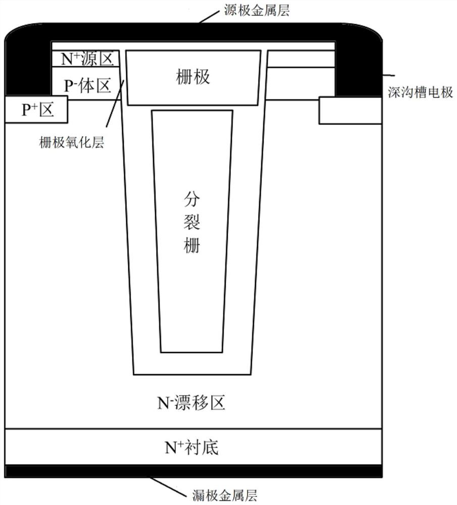
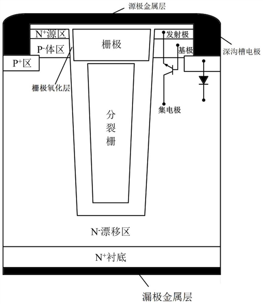
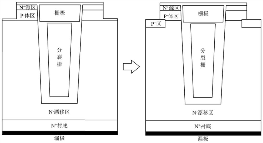
[0020] as attached figure 1 As shown, in this embodiment, a 100V shielded gate power MOSFET device is selected to simulate and verify the technical effect of the present invention. An anti-single event burnout str...


PUM

PropertyMeasurementUnit
radiusaaaaaaaaaa

Abstract

The invention discloses an anti-single event burning structure suitable for power semiconductor devices, which includes an epitaxial layer, an active region and a gate structure are arranged on the first main surface of the epitaxial layer, and the active region and the gate structure are A gate metal layer is provided; a substrate layer is provided on the second main surface of the epitaxial layer, and a drain metal layer is provided on the substrate layer; the epitaxial layer between the active region and the substrate layer forms a drift region ; The active region is provided with a vertical deep trench, and a source metal layer is provided in the deep trench; a P-type region is provided at the bottom of the source metal layer; the present invention is caused by heavy ions when the device is turned off. The transient current is mainly discharged through the deep trench electrode, which greatly reduces the transient current acting on the parasitic BJT, making it difficult for the parasitic BJT to conduct, thereby effectively improving the anti-SEB performance of the power semiconductor device; and the deep trench electrode The introduction of will not have any impact on the device channel region and reverse withstand voltage region, so the basic electrical characteristics of the device will not be affected in any way.

Description

technical field [0001] The invention relates to the anti-radiation strengthening technology of power semiconductor devices, in particular to an anti-single event burning structure suitable for power semiconductor devices. Background technique [0002] Power semiconductor devices have the advantages of large driving current, high breakdown voltage, fast speed, low power consumption, and large output power. They can realize power control and conversion in different ranges, and are widely used in power management of satellites and spacecraft. The field of application has enormous potential for development. Power semiconductor devices usually have the characteristics of small size and high operating voltage, and their working stability is easily affected by the natural radiation environment in space, especially the single event burnout (SEB) effect. SEB is usually induced by the radiation of heavy ions, which can generate a very high concentration of electron-hole pairs along t...

Claims


Application Information

Patent Timeline
Patent Type & Authority Patents(China)
IPC IPC(8): H01L23/552H01L29/78
CPCH01L23/552H01L29/7804H01L29/7813
Inventor 王颖于成浩曹菲包梦恬
Owner HANGZHOU DIANZI UNIV
Why Eureka
Try Eureka