Electron transport layer, light emitting device and preparation method thereof
An electron transport layer and light-emitting device technology, which is applied in the fields of electric solid-state devices, semiconductor/solid-state device manufacturing, electrical components, etc., can solve the problems of reducing the light-emitting performance of quantum dot thin films, and achieve the effects of good electrical stability and improved service life.
- Summary
- Abstract
- Description
- Claims
- Application Information
AI Technical Summary
Problems solved by technology
Method used
Image
Examples
preparation example Construction
[0042] The present invention also provides a preparation method of the above-mentioned light-emitting device:
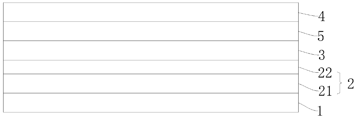
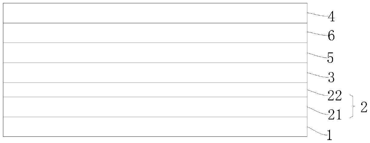
[0043] When the light-emitting device is an inverted device, the preparation method is as follows: providing a first electrode 1, setting a zinc oxide nanocrystal solution on the first electrode 1, forming a zinc oxide nanocrystal film 21 after drying, and forming a zinc oxide nanocrystal film 21 on the zinc oxide nanocrystal film 21. Deposit a layer of zinc oxide deposition film 22, prepare a light-emitting layer 3 on the zinc oxide deposition film 22, optionally set a hole transport layer 5 and / or a hole injection layer 6 on the light-emitting layer 3, and then set the second electrode 4;
[0044] When the light-emitting device is a positive-type device, the preparation method is to provide a second electrode 4, optionally arrange a hole injection layer 6 and / or a hole transport layer 5 on the second electrode 4, and then prepare a light-emitting layer 3, in A zin...
Embodiment 1
[0050] Fabrication of Inverse Light Emitting Devices
[0051] (1) Clean the anode ITO (indium tin oxide) with a thickness of 180nm: ultrasonically clean with ethanol, deionized water and acetone for 10min, and then use N 2 The liquid adhering to the ITO surface was blown dry, and treated with oxygen plasma for 10 minutes to remove impurities on the ITO surface to obtain a clean ITO transparent conductive glass.
[0052] (2) Make zinc oxide nanocrystal film: spin-coat zinc oxide nanocrystal solution (zinc oxide nanocrystal is Zn 0.85 Mg 0.15 O nanocrystals, the solvent is ethanol, the concentration is 30mg / mL), and the spin coating time is 50s. After the spin coating is completed, it is annealed at 120°C for 30min in the glove box, and finally a layer of zinc oxide nanocrystal film is formed on the ITO surface.
[0053] (3) Manufacture of zinc oxide deposited film: the composition of Zn was prepared on the zinc oxide nanocrystalline film by radio frequency sputtering process....
Embodiment 2
[0058] Fabrication of positive light-emitting devices
[0059] (1) Clean the anode ITO (indium tin oxide) with a thickness of 180nm: ultrasonically clean with ethanol, deionized water and acetone for 10min, and then use N 2 The liquid adhering to the ITO surface was blown dry, and treated with oxygen plasma for 10 minutes to remove impurities on the ITO surface to obtain a clean ITO transparent conductive glass.
[0060] (2) Make the hole injection layer and the hole transport layer: In the air environment, spin-coat PEDOT:PSS (polystyrene sulfonic acid solution) at a speed of 4000 rpm on the clean ITO transparent conductive glass, time After the spin coating is completed, it is annealed at 150°C in the air for 30 minutes, then transferred to a glove box in a nitrogen atmosphere, annealed at 130°C for 20 minutes, and finally forms a layer of PEDOT:PSS layer on the surface of ITO, namely Form a hole injection layer; then spin-coat poly((9,9-dioctylfluorene-2,7-diyl)-co(4,4'-( ...
PUM
 Abstract
Description
Claims
Application Information
 - R&D
- Intellectual Property
- Life Sciences
- Materials
- Tech Scout
- Unparalleled Data Quality
- Higher Quality Content
- 60% Fewer Hallucinations
Browse by: Latest US Patents, China's latest patents, Technical Efficacy Thesaurus, Application Domain, Technology Topic, Popular Technical Reports.
© 2025 PatSnap. All rights reserved.Legal|Privacy policy|Modern Slavery Act Transparency Statement|Sitemap|About US| Contact US: help@patsnap.com


