A method for manufacturing high-strength bumps on cof substrates

A manufacturing method and high-strength technology, applied in semiconductor/solid-state device manufacturing, electrical components, circuits, etc., can solve the problems of longer electroplating processing time and lower production efficiency, so as to reduce height deviation, improve production efficiency, and reduce The effect of height bias

Active Publication Date: 2021-03-30
江苏上达半导体有限公司
View PDF5 Cites 0 Cited by
  • Summary
  • Abstract
  • Description
  • Claims
  • Application Information

AI Technical Summary

Problems solved by technology

Therefore, the plating processing time will become longer and the production efficiency will decrease

Method used


Image

  • A method for manufacturing high-strength bumps on cof substrates
  • A method for manufacturing high-strength bumps on cof substrates
  • A method for manufacturing high-strength bumps on cof substrates

Examples


Embodiment Construction

[0040] The following will clearly and completely describe the technical solutions in the embodiments of the present invention with reference to the accompanying drawings in the embodiments of the present invention. Obviously, the described embodiments are only some, not all, embodiments of the present invention. Based on the embodiments of the present invention, all other embodiments obtained by persons of ordinary skill in the art without creative efforts fall within the protection scope of the present invention.

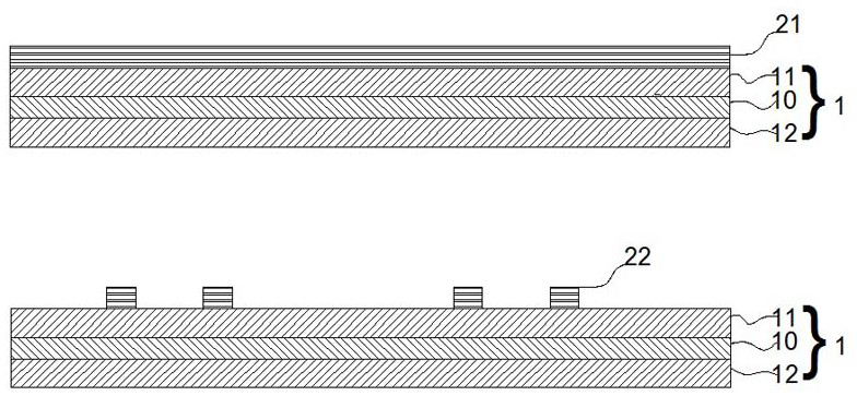
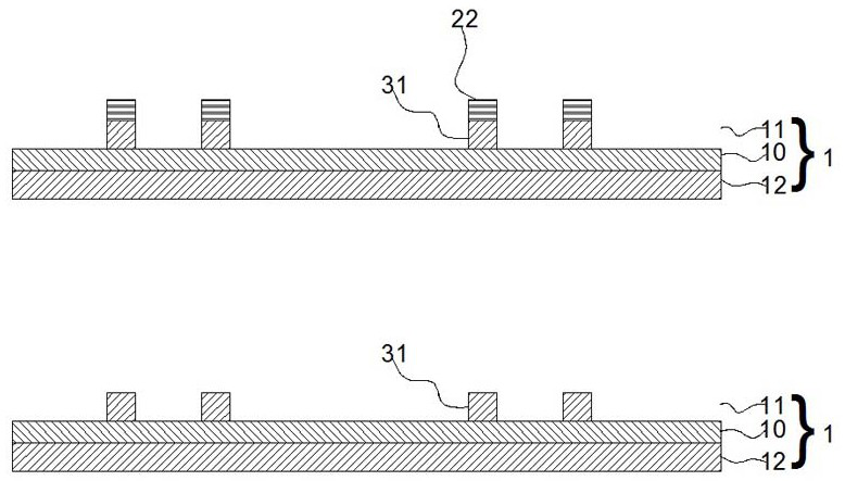
[0041] combine Figure 1 to Figure 12 As shown, a method for manufacturing a high-strength bump on a COF substrate is characterized in that it includes:

[0042] In the first photoresist process, photoresist 21 is coated on the copper foil 11 of the insulating substrate 1, and the insulating substrate 1 coated with photoresist 21 is exposed using a film negative, and the required photoresist pattern 22 is developed. reserve;

[0043] In the first etching process,...


PUM

PropertyMeasurementUnit
sizeaaaaaaaaaa

Abstract

The invention relates to a manufacturing method of a high-strength bump of a COF substrate, and belongs to the technical field of COF substrates. According to the invention, a first photoresist process, a first etching process, wet full etching, a second photoresist process, a second etching process, a press-fitting process, a third photoresist process, a third etching process, a copper electroplating process, a fourth photoresist process and a nickel-gold electroplating process are sequentially carried out. Compared with a bump formed according to the traditional electroplating treatment, theheight deviation of the bump is reduced. Even if the same electroplating treatment is performed, the height deviation of the bump is reduced in the case of electroless plating than in the case of electrolytic plating. The growth rate of the plating layer is likely to fluctuate due to the concentration of the current and the like in the electrolytic plating. The phenomenon does not occur under thecondition of electroless plating, and the plating layer can be uniformly grown on the whole. Compared with a bump formed by the traditional electroplating treatment, the height deviation of the bumpcan be reduced, and the production efficiency is improved.

Description

technical field [0001] The invention relates to a method for manufacturing high-strength bumps of a COF substrate, belonging to the technical field of COF substrates. Background technique [0002] With the continuous development of science and technology, electronic products are increasingly developing in the direction of miniaturization, intelligence, high performance and high reliability. The packaging substrate is transitioning from FPC to COF. The PTCH value of the COF substrate is getting smaller and smaller, and the pins in the packaging are becoming more and more dense and precise. The integrated circuit packaging not only directly affects the integration of integrated circuits, electronic modules and even the whole machine. Performance, but also restricts the miniaturization, low cost and reliability of the entire electronic system. With the gradual reduction of the size of the integrated circuit chip and the continuous improvement of the integration level, the elec...

Claims


Application Information

Patent Timeline
Patent Type & Authority Patents(China)
IPC IPC(8): H01L21/48
CPCH01L21/4846H01L21/4853
Inventor 戚爱康王健计晓东孟庆园孙彬沈洪李晓华
Owner 江苏上达半导体有限公司
Why Eureka
Try Eureka