
Magnetic storage element, and electronic device

A magnetic storage and component technology, applied in the parts of electromagnetic equipment, information storage, electrical components, etc., can solve problems such as read interference, and achieve the effect of reducing write current

Pending Publication Date: 2019-11-26
SONY SEMICON SOLUTIONS CORP
View PDF6 Cites 1 Cited by
  • Summary
  • Abstract
  • Description
  • Claims
  • Application Information

AI Technical Summary

Problems solved by technology

[0006] However, in fact, since the amount of current used to write and read information in STT-MRAM is close to each other, it is possible to cause read disturbance, that is, rewrite the stored information while reading information

Method used


Image

  • Magnetic storage element, and electronic device
  • Magnetic storage element, and electronic device
  • Magnetic storage element, and electronic device

Examples


Embodiment Construction

[0029] Hereinafter, preferred embodiments of the present disclosure are described in detail with reference to the accompanying drawings. It is to be noted that, in this specification and the drawings, components having substantially the same functional configuration are denoted by the same reference numerals, and thus descriptions of these components are omitted. Also, in this specification, the stacking direction of each layer is indicated as an upward direction.

[0030] Note that description is made in the following order.

[0031] 1. Overview of SOT-MRAM

[0032] 1.1. Technical background related to this disclosure

[0033] 1.2. The structure of SOT-MRAM

[0034] 1.3. Operation of SOT-MRAM

[0035] 2. Regarding an embodiment of the present disclosure

[0036] 2.1 First configuration

[0037] 2.2 The second configuration

[0038] 2.3 The third configuration

[0039] 2.4 The fourth configuration

[0040] 3. Configuration of electronic equipment

[0041]

[0042] ...


PUM

PropertyMeasurementUnit
thicknessaaaaaaaaaa

Abstract

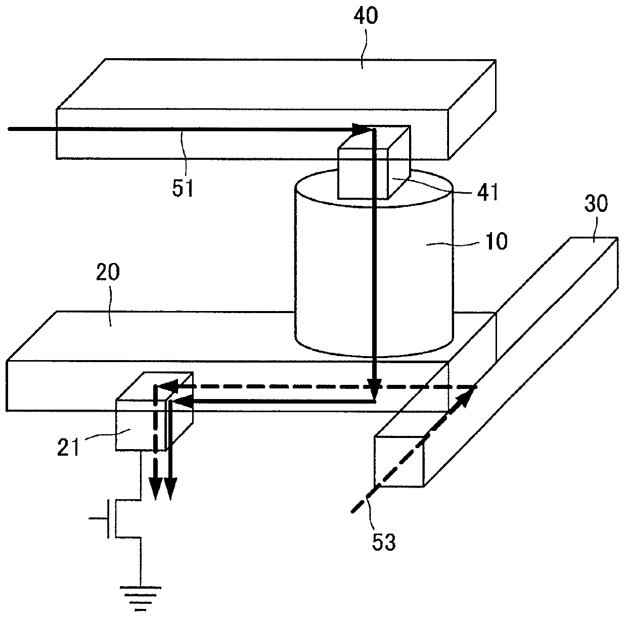
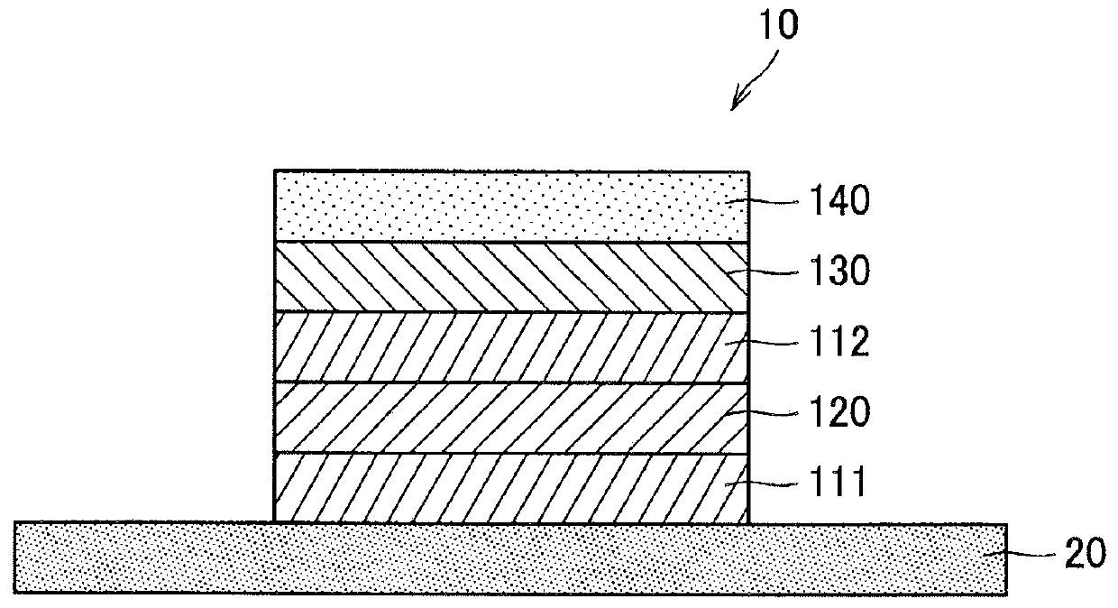
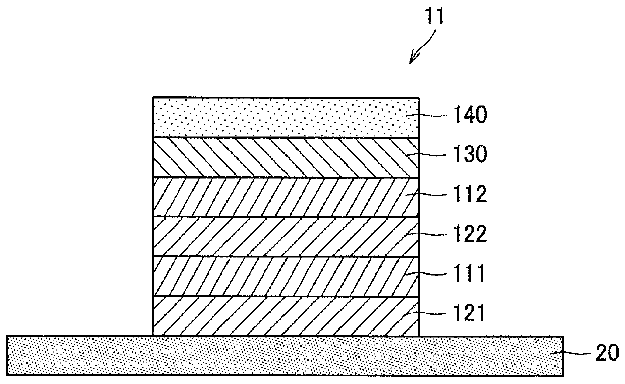
To provide a magnetic storage element in which a writing current is reduced while maintaining the magnetism-retaining characteristics of a storage layer; and an electronic device. A magnetic storage element, provided with: a spin orbit layer extended in one direction; a write line electrically connected to the spin orbit layer, the write line channeling a current in the extension direction of thespin orbit layer; a tunnel junction element provided on the spin orbit layer by laminating a memory layer, an insulator layer, and a magnetization fixed layer in the stated order; and a non-magnetic layer having a film thickness of 2 nm or below, the non-magnetic layer being provided at one of the lamination positions between the spin orbit layer and the insulator layer.

Description

technical field [0001] The present disclosure relates to a magnetic memory element and an electronic device. Background technique [0002] With the continuous improvement of the performance of various information equipment, the built-in storage devices in various information equipment also show the improvement of integration, the improvement of speed and the reduction of power consumption. Accordingly, the performance of memory elements using semiconductors is also improving. [0003] For example, flash memory rather than hard drive devices are becoming more and more popular as mass file storage. In addition, various types of storage elements such as FeRAM (Ferroelectric Random Access Memory), PCRAM (Phase Change Random Access Memory) or MRAM (Magnetic Random Access Memory) instead of NOR type flash memory and DRAM (Dynamic Random Access Memory) Access memory), is being developed as code storage or working memory. [0004] For example, MRAMs, in which information is store...

Claims


Application Information

Patent Timeline
Patent Type & Authority Applications(China)
IPC IPC(8): H01L21/8239H01L27/105H01L29/82H01L43/08H10N50/01H10N50/10H10N50/80
CPCH01L29/82G11C11/161G11C11/1675Y02D10/00H10N50/10G01R33/093H10B61/22H10N50/01H10N50/80H10N50/85H10B61/00
Inventor 长谷直基细见政功肥后丰大森广之内田裕行佐藤阳
Owner SONY SEMICON SOLUTIONS CORP
Learn More