A full adder based on spin-orbit moment

A spin-orbit and spin-orbit coupling technology, used in magnetic field-controlled resistors, instruments, static memories, etc., can solve the problems of high data transfer overhead and high static power consumption of CMOS full adders, and avoid the data transfer process. , The effect of solving the problem of static power consumption

Active Publication Date: 2021-05-25
BEIHANG UNIV
View PDF5 Cites 0 Cited by
  • Summary
  • Abstract
  • Description
  • Claims
  • Application Information

AI Technical Summary

Problems solved by technology

[0009] Aiming at the problems of high static power consumption and high data transfer overhead of the current CMOS full adder mentioned in the above background, the present invention provides a full adder based on spin-orbit moment

Method used


Image

  • A full adder based on spin-orbit moment
  • A full adder based on spin-orbit moment
  • A full adder based on spin-orbit moment

Examples


Embodiment Construction

[0068] The substantive features of the present invention are further described with reference to the accompanying drawings. Detailed exemplary embodiments are disclosed herein, specific structural and functional details thereof are merely representative for purposes of describing exemplary embodiments, therefore, the invention may be embodied in many alternative forms and should not be construed To be limited only to the exemplary embodiments set forth herein, all changes, equivalents, and alternatives falling within the scope of the invention should be covered. Additionally, well-known elements, devices and subcircuits of the invention will not be described in detail or will be omitted so as not to obscure the relevant details of the embodiments of the invention.

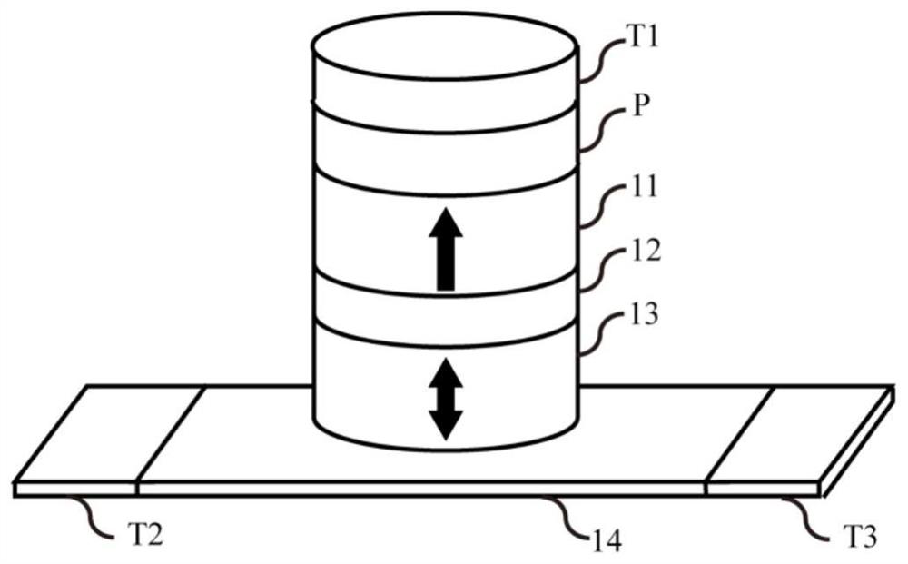
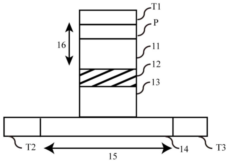
[0069] Figure 1A Schematic diagram of the structure of a spin-orbit moment magnetic tunnel junction device; Figure 1B Circuit symbol diagram for the device.

[0070] like Figure 1A As shown, the spin-orbit mom...


PUM


Abstract

The invention discloses a spin-orbit moment-based full adder, which is a cascaded structure composed of a spin-orbit moment magnetic tunnel junction and a CMOS transistor. Each stage includes an addition operation module, a carry operation module, a data storage module and timing control module. The operation method of the full adder includes: the first addition operation: perform the addition operation of the addend and the addend of each bit, and store the operation result of the bit in the magnetic tunnel junction in a non-volatile form; One carry operation: carry out the first carry signal calculation through the carry circuit to obtain the carry result of the operation at this stage; the second addition operation: deal with the influence of low-order carry on the result of the addition operation at this stage; the second carry operation: pass The carry circuit in a carry operation handles the influence of the low-order carry on the carry result of the current stage; the carry signal is passed to the full adder of the next stage to repeat the operation of the previous steps. The invention has the advantages of low static power consumption and no data transfer process.

Description

【Technical field】 [0001] The invention relates to a spin-orbit moment-based full adder, which belongs to the field of integrated circuit design. 【Background technique】 [0002] The full adder is the basic functional module in the combinational logic circuit, and also the core of processing the addition operation in the central processing unit (CPU). According to the function of a full adder, the logical expression of the full adder can be obtained as follows: [0003] [0004] C0=XY+Ci(X+Y) [0005] Among them, X, Y and Ci respectively represent the input signal of the adder, X and Y represent the addend and the summand respectively, Ci is the low-order carry input signal, C0 is the output carry of the current stage, and S is the standard sum. [0006] The traditional full adder is designed using a complementary metal-oxide-semiconductor (CMOS) process, which has some disadvantages: first, the leakage current of the CMOS transistor increases with the decrease of the pro...

Claims


Application Information

Patent Timeline
Patent Type & Authority Patents(China)
IPC IPC(8): G06F7/501G11C11/16H01L43/08
CPCG06F7/501G11C11/161H10N50/10
Inventor 周浩昌刘桐汐王昭昊吴比赵巍胜
Owner BEIHANG UNIV
Why Eureka
Try Eureka