Logic expression extraction and switch level design method of CMOS transmission gate logic circuit
A logic expression, logic circuit technology, applied in computing, electrical digital data processing, special data processing applications, etc., can solve the problems of reduced process feature size and increased static power consumption of MOS transistors
- Summary
- Abstract
- Description
- Claims
- Application Information
AI Technical Summary
Problems solved by technology
Method used
Image


Examples
Embodiment 1
[0075] A logical expression extraction and switch-level design method for a CMOS transmission gate logic circuit expands the Boolean algebra system to obtain an extended Boolean algebra system; a corresponding switch-level signal flow graph model is established by the CMOS transmission gate logic circuit, thereby The equivalent signal flow graph model of the output function of the circuit is extracted from the model, and the switch-level function expression of the circuit is obtained by combining the switch-level signal flow graph model with the extended Boolean algebra system, and thus the CMOS transmission gate logic circuit is obtained.
[0076] The number of MOS tubes contained in the circuit is still an important indicator to measure the power consumption and area of the circuit. The study found that using the full-swing CMOS transmission gate circuit structure can avoid threshold voltage loss, reduce sub-threshold power consumption, and reduce the number of MOS transist...
Embodiment 2
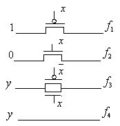
[0115] Such as figure 1 As shown, there are four types of component branches of the CMOS transmission gate circuit, namely, the PMOS tube branch, the NMOS tube branch, the CMOS transmission gate branch and the connection branch, wherein the PMOS tube and the NMOS tube are single-channel transmission gates, The 1 signal and the 0 signal can be transmitted without loss, respectively, and the CMOS transmission gate branch is a dual-channel transmission gate, which can transmit signal variables without loss. The above three types of branches are all controlled branches, and the connection branches are uncontrolled branches, that is, direct transmission (through) branches. The switch-level function expressions of the four types of component branches are respectively
[0116] f1 =x 0.5 ·[1],f 2 = 0.5 x[0], f 4 =U·[y]=[y]
[0117] Its corresponding switch-level signal flow graph model, such as figure 2 shown. The arrow on the branch indicates the transmission (flow) direct...
Embodiment 3
[0128] Such as Figure 7 As shown, the CMOS transmission gate type full adder circuit (the circuit name is EX2) obtained by using the switch-signal theory design method. Use the equivalent signal flow graph model method to find the logic function expression of the circuit.
[0129] Step1 modeling. Depend on Figure 7 For the full adder circuit shown, draw the signal flow graph model of the complement function of the output function of the circuit as Figure 8 shown. In the figure, C(0) means C=0, express etc. Depend on Figure 8 ,use and The signal flow diagram of the transmission 0 signal is transformed to obtain the output function s of the circuit i , c i and the equivalent signal flow graph model of h as Figure 9 shown.
[0130] Step2 analysis. Depend on Figure 9 The output s of the full adder can be obtained directly i and c i for
[0131]
[0132] After simplification by Boolean algebra (signal algebra) method, the logical expression of the ful...
PUM
 Abstract
Description
Claims
Application Information
 - R&D
- Intellectual Property
- Life Sciences
- Materials
- Tech Scout
- Unparalleled Data Quality
- Higher Quality Content
- 60% Fewer Hallucinations
Browse by: Latest US Patents, China's latest patents, Technical Efficacy Thesaurus, Application Domain, Technology Topic, Popular Technical Reports.
© 2025 PatSnap. All rights reserved.Legal|Privacy policy|Modern Slavery Act Transparency Statement|Sitemap|About US| Contact US: help@patsnap.com