
MRAM storage chip adopting fully-depleted insulated silicon FD-SOI field effect transistor

A technology of FD-SOI and memory chips, which is applied in the direction of information storage, static memory, digital memory information, etc., can solve the problems of field effect tubes not working normally, burning out, etc., and achieve the effect of solving insufficient driving current and eliminating latch-up effect

Active Publication Date: 2019-09-03
SHANGHAI CIYU INFORMATION TECH
View PDF11 Cites 0 Cited by
  • Summary
  • Abstract
  • Description
  • Claims
  • Application Information

AI Technical Summary

Problems solved by technology

This is because once the body potential of the back gate is raised in the bulk silicon field effect transistor, a current will be generated in the back gate of the back gate, and the two sets of sources, drains and back gates of the adjacent two NMOS and PMOS transistors A set of NPN and PNP triode loops will be formed in the pole, and the back gate current will be amplified by positive feedback, so that the field effect tube will not work properly or even have the risk of burning
In addition, if the source or drain is at 0 potential when the back gate potential is raised, the forward conduction of the PN junction will occur between the source or drain and the back gate, making the field effect transistor unable to work normally.

Method used


Image

  • MRAM storage chip adopting fully-depleted insulated silicon FD-SOI field effect transistor
  • MRAM storage chip adopting fully-depleted insulated silicon FD-SOI field effect transistor
  • MRAM storage chip adopting fully-depleted insulated silicon FD-SOI field effect transistor

Examples


Embodiment 1

[0036] An MRAM memory chip using a fully depleted silicon-on-insulator FD-SOI field effect transistor, the field effect transistor of each MRAM memory unit of the MRAM memory chip adopts a fully depleted silicon-on-insulator FD-SOI field effect transistor, such as Figure 5 shown. The MRAM chip also includes a body potential control unit, which regulates the body potential of the back gate of the memory chip.

[0037] Since the back gate body of the fully depleted silicon-on-insulator FD-SOI field effect transistor is isolated by a layer of silicon oxide dielectric layer between the source source and the drain drain, the MRAM chip is raised when the back gate is raised. When the body potential is used, PNP and NPN type triode structures will not be formed, and there will be no latch-up effect, which will not bring area and cost costs.

Embodiment 2

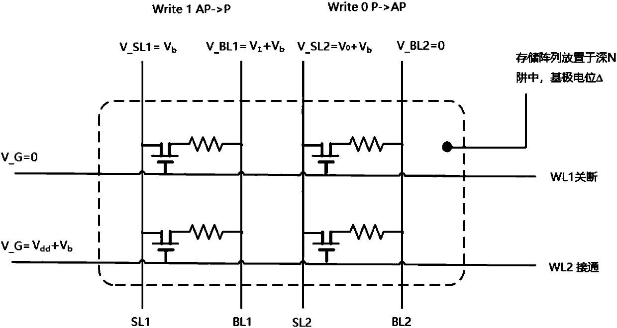
[0039] A design method for adjusting the body potential of the back gate of an MRAM memory chip using a fully depleted silicon-on-insulator FD-SOI field effect transistor, such as Figure 6 and Figure 7 As shown, the specific design method is as follows:

[0040] The back gate body potential is set to V_body=V b , V bThe value can be flexibly set according to design needs. Preferably, the body potential of the back gate can be reasonably adjusted under different operations through the back gate body potential control circuit.

[0041] During a read operation, take V b =0.

[0042] The specific method for adjusting the body potential of the back gate of the MRAM memory chip is as follows:

[0043] When writing 0 direction:

[0044] The source line potential V_SL is set to V 0 +V b , the bit line potential V_BL is set to 0, and the gate (word line) potential V_G is set to V dd +V b . Among them, V 0 +V b is the voltage signal that the read drive circuit needs to g...


PUM


Abstract

The invention discloses an MRAM storage chip adopting a fully-depleted insulated silicon FD-SOI field effect transistor and a design method for adjusting grid potential. A fully-depleted insulated silicon FD-SOI field effect transistor is adopted as a field effect transistor of each MRAM storage unit of the MRAM storage array chip, and the MRAM storage array chip comprises a bulk potential controlunit. In a working state, the value Vb of the back gate potential V _ body of the FD-SOI field effect transistor can be flexibly configured to be any value in a proper range. When the design method writes in the 0 direction, the potential V _ SL of a source line is set to be V0 + Vb, the potential V _ BL of a bit line is set to be 0, and the potential V _ G of a grid electrode (word line) is setto be Vdd + Vb. In the 1-direction writing process, the source line potential V _ SL is set to be Vb, the bit line potential V _ BL is set to be V1 + Vb, and the grid electrode (word line) potential V_ G is set to be Vdd + Vb. The latch-up effect of the bulk silicon field effect transistor can be eliminated, the potential of the back gate can be adjusted, and the problem of insufficient driving current provided by a writing circuit is solved.

Description

technical field [0001] The invention belongs to the technical field of semiconductor chip storage, and in particular relates to an MRAM memory chip using a fully depleted insulating silicon FD-SOI field effect transistor. Background technique [0002] Magnetic Random Access Memory (MRAM) is an emerging non-volatile storage technology. It has high-speed read and write speed and high integration, and can be rewritten infinitely. MRAM can be read and written as fast as SRAM / DRAM, and can permanently retain data after power failure like Flash memory. [0003] MRAM has very good economy and performance. Its silicon chip area occupied per unit capacity has great advantages over SRAM, and also has advantages over NOR Flash, which is often used in such chips, and has greater advantages than embedded NOR Flash. . The MRAM read and write delay is close to the best SRAM, and the power consumption is the best among various memory and storage technologies; and MRAM is compatible with ...

Claims


Application Information

Patent Timeline
Patent Type & Authority Applications(China)
IPC IPC(8): G11C11/16
CPCG11C11/1673G11C11/1675
Inventor 叶力戴瑾
Owner SHANGHAI CIYU INFORMATION TECH
Learn More