Novel lithium niobate optical waveguide wafer and preparation method thereof
An optical waveguide, lithium niobate technology, which is applied to optical waveguides, light guides, optics, etc., can solve the problems of complex preparation process, high preparation cost, low yield, etc., and achieves high light damage threshold, simple preparation process, and yield. high effect
- Summary
- Abstract
- Description
- Claims
- Application Information
AI Technical Summary
Problems solved by technology
Method used
Image

Examples
Embodiment 1
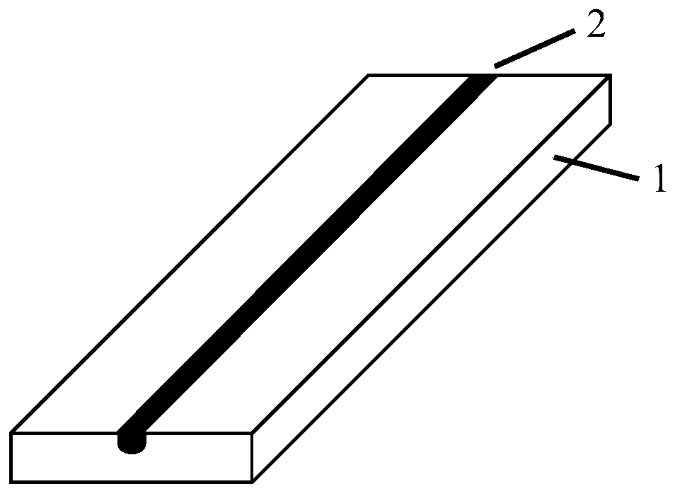
[0049] Such as figure 1 As shown, this embodiment provides a novel lithium niobate optical waveguide chip, including: a lithium niobate chip 1 and an optical waveguide 2;
[0050] The lithium niobate wafer 1 adopts an optical grade crystal, and its crystal orientation is one of four types: X-cut Y-pass or X-cut Z-pass or Y-cut Z-pass or Z-cut Y-pass;
[0051] The optical waveguide 2 is zinc oxide diffused lithium niobate optical waveguide, the waveguide width is 1 μm to 20 μm, and the waveguide depth is 1 μm to 20 μm.
[0052] Preferably, in order to utilize the maximum electro-optic coefficient γ of lithium niobate crystal 33 , the crystal orientation of the lithium niobate wafer 1 is selected as X-cut Y-pass or Z-cut Y-pass.
[0053] Preferably, the lithium niobate wafer 1 has a thickness of 0.1 mm to 2 mm.
[0054] Preferably, the lithium niobate wafer 1 has a thickness of 0.5 mm or 1 mm.
Embodiment 2
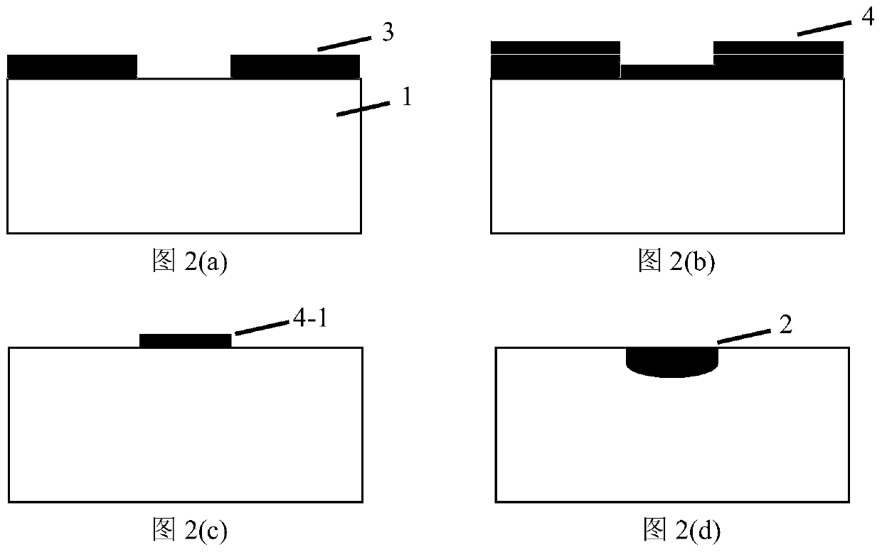
[0056] Such as figure 2 As shown, the present embodiment provides a manufacturing method of the novel lithium niobate optical waveguide wafer in Embodiment 1, and the flow chart of the manufacturing method is as follows figure 2 (a) to figure 2 (d), specifically include the following steps:
[0057] Step 1: using the conventional photolithography technology in the semiconductor process, a photoresist mask 3 with a pattern of the optical waveguide 2 is fabricated on the surface of the lithium niobate wafer 1;
[0058] Step 2: Prepare a layer of zinc oxide film 4 with a thickness of 10nm to 150nm on the photoresist mask by using one of the coating techniques such as electron beam evaporation or magnetron sputtering or ion sputtering;
[0059] Step 3: leave a strip-shaped zinc oxide film 4-1 with an optical waveguide 2 pattern on the surface of the lithium niobate wafer 1 through a lift-off process, the thickness of the strip-shaped zinc oxide film 4-1 is 10nm to 150nm, and ...
Embodiment 3
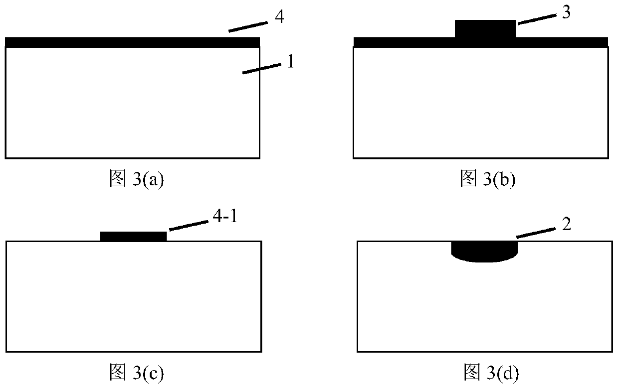
[0062] Such as image 3 As shown, the present embodiment provides another manufacturing method of the novel lithium niobate optical waveguide wafer in Embodiment 1, and the flow chart of the manufacturing method is as follows image 3 (a) to image 3 (d), specifically include the following steps:
[0063] Step 1: Prepare a zinc oxide film 4 with a thickness of 10nm to 150nm on the surface of the lithium niobate wafer 1 by using one of the coating techniques such as electron beam evaporation or magnetron sputtering or ion sputtering;
[0064] Step 2: Fabricate a photoresist mask 3 with a pattern of the optical waveguide 2 on the surface of the zinc oxide film 4 by photolithography;
[0065] Step 3: Corroding or etching the area other than the photoresist mask 3 by wet etching or dry etching, and leaving the strip-shaped oxidation of the optical waveguide 2 pattern on the surface of the lithium niobate wafer 1 The zinc thin film 4-1, the strip-shaped zinc oxide thin film 4-1 ...
PUM
 Abstract
Description
Claims
Application Information
 - R&D
- Intellectual Property
- Life Sciences
- Materials
- Tech Scout
- Unparalleled Data Quality
- Higher Quality Content
- 60% Fewer Hallucinations
Browse by: Latest US Patents, China's latest patents, Technical Efficacy Thesaurus, Application Domain, Technology Topic, Popular Technical Reports.
© 2025 PatSnap. All rights reserved.Legal|Privacy policy|Modern Slavery Act Transparency Statement|Sitemap|About US| Contact US: help@patsnap.com