Multi-layer composite protection layer applied to PCB and method
A multi-layer composite and protective layer technology, applied in the direction of coating non-metallic protective layer, secondary treatment of printed circuit, electrical components, etc., can solve the problems of easily damaged electronic components, long curing time of colloid, occupying structural space, etc. Achieve the effects of improved waterproof performance and anti-corrosion performance, strong physical and mechanical protection performance, and strong adhesion
- Summary
- Abstract
- Description
- Claims
- Application Information
AI Technical Summary
Problems solved by technology
Method used
Image
Examples
Embodiment 1
[0039] (1) First, use xylene to clean the PCB and components, and clean the rosin, flux, oil and other sundries on the surface of the PCB.
[0040](2) The PCB is baked in an oven using a dehumidification process, and the moisture absorbed by the PCB and components during the storage and circulation process is discharged.
[0041] (3) Immerse the PCB in the nanomaterial silica solution. After the surface of the PCB is completely debubbled, take out the PCB and dry it.
[0042] (4) A vacuum coating machine is used to vacuum coat the PCB by chemical vapor deposition. Among them, the coating machine and coating materials are all used in Shanghai Paraleng Coating Machine, using Paryleng C material. Coating thickness is 30um.
[0043] (5) Immerse the PCB in epoxy resin, repeatedly immerse in YF-3508 epoxy resin, the thickness is about 0.5mm, and wait for the colloid to solidify.
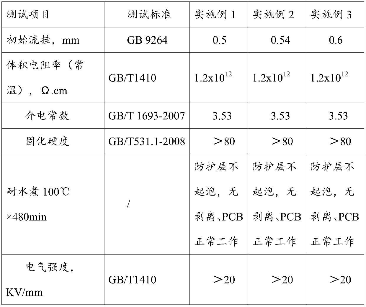
[0044] The above-mentioned composite protective layer was tested, and the results are shown in Table...
Embodiment 2
[0049] (1) First, use xylene to clean the PCB and components, and clean the rosin, flux, oil and other sundries on the surface of the PCB.
[0050] (2) The PCB is baked in an oven using a dehumidification process, and the moisture absorbed by the PCB and components during the storage and circulation process is discharged.
[0051] (3) Immerse the PCB in a nanomaterial silica solution with a particle size of 7-30nm. After the surface of the PCB is completely debubbled, take out the PCB and let it dry for 3-5 minutes to obtain a film layer of 500-1000nm.
[0052] (4) A vacuum coating machine is used to vacuum coat the PCB by chemical vapor deposition. Among them, the coating machine and coating materials are all used in Shanghai Paraleng Coating Machine, using Paryleng C material. Coating thickness is 35um.
[0053] (5) Immerse the PCB in epoxy resin, repeatedly immerse in YF-3508 epoxy resin, the thickness is about 0.7mm, and wait for the colloid to solidify.
Embodiment 3
[0055] (1) First, use xylene to clean the PCB and components, and clean the rosin, flux, oil and other sundries on the surface of the PCB.
[0056] (2) The PCB is baked in an oven using a dehumidification process, and the moisture absorbed by the PCB and components during the storage and circulation process is discharged.
[0057] (3) Immerse the PCB in a nanomaterial silica solution with a particle size of 7-30. After the surface of the PCB is completely debubbled, take out the PCB and let it dry for 3-5 minutes to obtain a film layer of 500-1000nm.
[0058] (4) A vacuum coating machine is used to vacuum coat the PCB by chemical vapor deposition. Among them, the coating machine and the coating material are all used in the coating machine of Shanghai Paraleng, and the material of Paryleng C is used, and the coating thickness is 40um.
[0059] (5) Immerse the PCB in epoxy resin, repeatedly immerse in YF-3508 epoxy resin, the thickness is about 1mm, and wait for the colloid to ...
PUM
| Property | Measurement | Unit |
|---|---|---|
| Thickness | aaaaa | aaaaa |
| Particle size | aaaaa | aaaaa |
| Thickness | aaaaa | aaaaa |
Abstract
Description
Claims
Application Information
 - R&D Engineer
- R&D Manager
- IP Professional
- Industry Leading Data Capabilities
- Powerful AI technology
- Patent DNA Extraction
Browse by: Latest US Patents, China's latest patents, Technical Efficacy Thesaurus, Application Domain, Technology Topic, Popular Technical Reports.
© 2024 PatSnap. All rights reserved.Legal|Privacy policy|Modern Slavery Act Transparency Statement|Sitemap|About US| Contact US: help@patsnap.com


