
Drive circuit of silicon carbide semiconductor field effect transistor

A field-effect transistor and driving circuit technology, applied in the field of driving circuits of silicon carbide semiconductor field-response transistors, can solve the problem that high turn-off speed and low voltage spikes of SiCMOSFET cannot be realized at the same time, so as to reduce voltage spikes, save costs, The effect of speeding up the descent

Inactive Publication Date: 2019-08-09
HUAZHONG UNIV OF SCI & TECH
View PDF5 Cites 9 Cited by
  • Summary
  • Abstract
  • Description
  • Claims
  • Application Information

AI Technical Summary

Problems solved by technology

[0004] The invention provides a driving circuit of a silicon carbide semiconductor field-sensing transistor, which is used to solve the technical problem that the existing SiC MOSFET driving circuit cannot realize the high turn-off speed and low voltage peak of SiC MOSFET at the same time

Method used


Image

  • Drive circuit of silicon carbide semiconductor field effect transistor
  • Drive circuit of silicon carbide semiconductor field effect transistor
  • Drive circuit of silicon carbide semiconductor field effect transistor

Examples


Embodiment 1

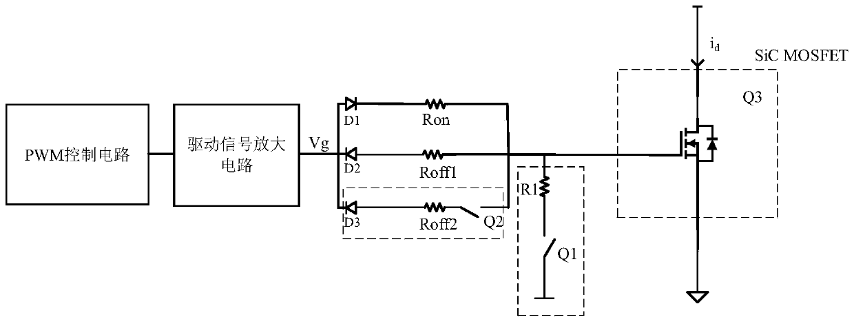
[0036] A driving circuit 100 for a silicon carbide semiconductor field effect transistor, such as figure 1 As shown, it includes: PWM control circuit, drive signal amplification circuit, shutdown circuit, gate shunt circuit and current change rate control circuit. Among them, the output end of the PWM control circuit is connected with the input end of the driving signal amplifying circuit, and is used to control the output driving voltage of the driving signal amplifying circuit; the output end of the shut-off circuit is connected with the output end of the driving signal amplifying circuit, and the input end is connected with the SiC MOSFET The gate connection is used to turn off the turned-on SiC MOSFET; the control terminal of the gate shunt circuit is connected to the output terminal of the driving signal amplifier circuit, and the input terminal is connected to the gate, which is used to turn on when the shutdown circuit is working , to shunt the gate current of the SiC M...


PUM


Abstract

The invention discloses a drive circuit of a silicon carbide semiconductor field effect transistor. The drive circuit comprises a PWM control circuit, a drive signal amplification circuit, a turn-offcircuit, a gate shunt circuit and a current change rate control circuit, wherein the gate shunt circuit is switched on when the turn-off circuit works to perform shunt of the gate current of a SiC MOSFET (Metal-Oxide-Semiconductor Field-Effect Transistor) and accelerate the switch-off of the SiC MOSFET; the SiC MOSFET is switched off when the drain-source voltage of the SiC MOSFET is increased toa preset value; the current change rate control circuit is switched off when the drain-source voltage of the SiC MOSFET is increased to the preset value to reduce the leakage current change rate. Thegate shunt circuit is arranged to perform shunt of the gate output current in the SiC MOSFET switch-off process and speed up the decreasing speed of the gate-source voltage so as to improve the switch-off speed of the SiC MOSFET; and besides, in the switch-off process of the SiC MOSFET, the switch-off of the current change rate control circuit reduces the leakage current change rate so as to reduce the voltage peak when the SiC MOSFET is switched off, the two circuits cooperatively act to achieve the voltage reduction speed and the low-voltage peak of the high gate-source voltage and ensure the safety operation of the SiC MOSFET.

Description

technical field [0001] The invention belongs to the field of power electronics driving, and more specifically relates to a driving circuit of a silicon carbide semiconductor field-effect transistor. Background technique [0002] SiC MOSFET (Metal-Oxide-Semiconductor Field-Effect Transistor) is a silicon carbide metal-oxide semiconductor field effect transistor, which has the advantages of fast switching speed, low switching loss, good temperature performance, high withstand voltage level, and small size. The field of electronic converters has very good application prospects. High frequency is the development trend of power electronic conversion technology. However, due to the fast switching speed of SiC MOSFET, it is easily affected by various parasitic parameters in high frequency applications, resulting in oscillation and false conduction. Therefore, in practical applications, corresponding driving circuits must be designed to ensure the safe and reliable operation of SiC...

Claims


Application Information

Patent Timeline
Patent Type & Authority Applications(China)
IPC IPC(8): H02M1/08
CPCH02M1/08Y02B70/10
Inventor 孔武斌高学鹏高慧达常亮甘醇曲荣海
Owner HUAZHONG UNIV OF SCI & TECH
Learn More