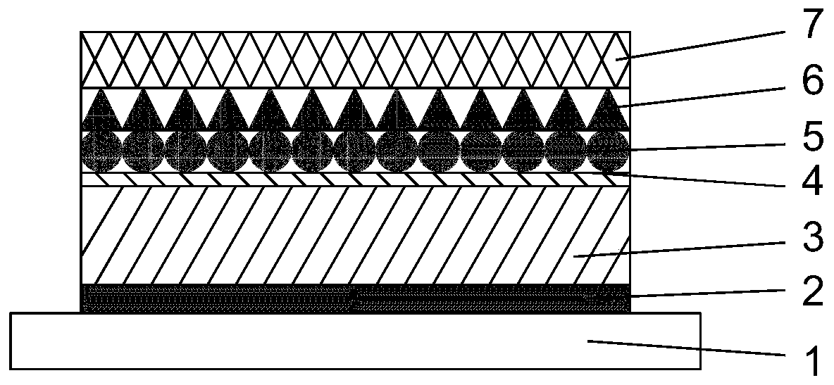
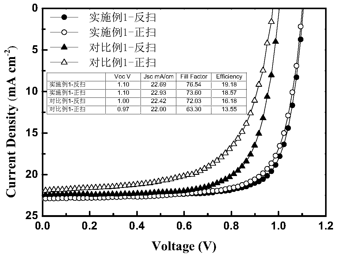
Non-fullerene perovskite solar cell and preparation method thereof
A technology of fullerene perovskite and solar cells, applied in circuits, photovoltaic power generation, electrical components, etc., can solve problems such as poor stability and low photoelectric conversion efficiency, achieve improved photoelectric efficiency, excellent electron mobility, and reduce hysteresis Effect
- Summary
- Abstract
- Description
- Claims
- Application Information
AI Technical Summary
Problems solved by technology
Method used
Image
Examples
Embodiment 1
[0060] The silicon phthalocyanine used in this embodiment is a compound of formula (3):
[0061]
[0062] (1) Pretreatment of conductive substrate: the use specification is light transmittance> 85% square value <10Ω, 15mm*15mm conductive ITO is used as the device substrate. After the conductive substrate is soaked in detergent for 24 hours, use deionized water, acetone and isopropanol in an ultrasonic cleaner for 10 minutes, then use deionized water Rinse, then dry with nitrogen flow, after drying, the conductive substrate is treated with ultraviolet ozone for 12 minutes before use;
[0063] (2) Preparation of hole transport layer: use PTAA material as the hole transport layer, weigh the PTAA mass to 1.5mg, dissolve it in 10ml chlorobenzene solvent, heat and dissolve it on a heating stage at 65℃ for 8h, and spin-coating after it is fully dissolved On the ITO substrate after UV treatment, the rotation speed is 6000rpm, the time is 30s, and the drying is at 65℃ during spin coating;
...
Embodiment 2
[0070] The silicon phthalocyanine used in this embodiment is a compound of formula (4):
[0071]
[0072] (1) Pretreatment of conductive substrate: the use specification is light transmittance> 85% square value <10Ω, 15mm*15mm conductive ITO is used as the device substrate. After the conductive substrate is soaked in detergent water for 24 hours, it is sonicated with deionized water, acetone and isopropanol in an ultrasonic cleaner for 15 minutes, and then deionized Rinse with water, then dry with nitrogen flow, after drying, the conductive substrate is treated with ultraviolet ozone for 15 minutes before use;
[0073] (2) Preparation of hole transport layer: use PTAA material as the hole transport layer, weigh the PTAA mass to 1.5mg, dissolve it in 10ml chlorobenzene solvent, heat and dissolve it on a heating stage at 65℃ for 8h, and spin-coating after it is fully dissolved On the ITO substrate after UV treatment, the rotation speed is 6000rpm, the time is 30s, and the drying is a...
Embodiment 3
[0080] The silicon phthalocyanine used in this embodiment is a compound of formula (5):
[0081]
[0082] (1) Pretreatment of conductive substrate: the use specification is light transmittance> 85% square value <10Ω, 15mm*15mm conductive ITO is used as the device substrate. After the conductive substrate is soaked in detergent for 24 hours, use deionized water, acetone and isopropanol in an ultrasonic cleaner for 10 minutes, then use deionized water Rinse, then dry with nitrogen flow, after drying, the conductive substrate is treated with ultraviolet ozone for 12 minutes before use;
[0083] (2) Preparation of hole transport layer: use PTAA material as the hole transport layer, weigh the PTAA mass to 1.5mg, dissolve it in 10ml chlorobenzene solvent, heat and dissolve it on a heating stage at 65℃ for 8h, and spin-coating after it is fully dissolved On the ITO substrate after UV treatment, the rotation speed is 6000rpm, the time is 30s, and the drying is at 65℃ during spin coating;
...
PUM
 Abstract
Description
Claims
Application Information
 - R&D
- Intellectual Property
- Life Sciences
- Materials
- Tech Scout
- Unparalleled Data Quality
- Higher Quality Content
- 60% Fewer Hallucinations
Browse by: Latest US Patents, China's latest patents, Technical Efficacy Thesaurus, Application Domain, Technology Topic, Popular Technical Reports.
© 2025 PatSnap. All rights reserved.Legal|Privacy policy|Modern Slavery Act Transparency Statement|Sitemap|About US| Contact US: help@patsnap.com


