Plane optical component surface quality rapid detecting device and method

A technology for optical components and surface quality, applied in the field of optical inspection, can solve the problem of not being able to obtain information on surface defects of large quantities of flat optical components in a short time.

Active Publication Date: 2019-07-05
SICHUAN UNIV
View PDF7 Cites 11 Cited by
  • Summary
  • Abstract
  • Description
  • Claims
  • Application Information

AI Technical Summary

Problems solved by technology

[0004] In order to solve the problem that the existing surface defect detection technology cannot obtain a large number of surface defect information of planar optical elements in a short time, the present invention proposes a rapid detection device for surface quality of planar optical elements based on total scattering measurement, specifically Including laser light source, beam splitter, laser beam expander, aperture stop, high reflection mirror, integrating sphere, CMOS image sensor, light collector, diffuse reflector, photodetector 1, photodetector 2, XY two-dimensional guideway , two-dimensional rotation system, Z guide rail, planar optical element; the planar optical element is fixed on the two-dimensional rotation system, and the two-dimensional rotation system is installed on the XY guide rail, so as to realize the multi-axis linkage of the planar optical element; the CMOS image sensor is connected to the outside The image processor is fixed on the bottom of the integrating sphere, the integrating sphere is fixed on the Z-guiding rail, and moves along the Z-axis along with the Z-guiding rail, the photodetector 2 is fixed at the detection hole of the integrating sphere; the photodetector 1 is placed In the detection optical path, combined with a laser beam splitter, real-time monitoring of the energy of the detection beam is realized

Method used


Image

  • Plane optical component surface quality rapid detecting device and method
  • Plane optical component surface quality rapid detecting device and method
  • Plane optical component surface quality rapid detecting device and method

Examples


Embodiment Construction

[0023] The following will clearly and completely describe the technical solutions in the embodiments of the present invention with reference to the drawings in the embodiments of the present invention. Apparently, the described embodiments are only some of the embodiments of the present invention, but not all of them. Based on the embodiments of the present invention, all other embodiments obtained by persons of ordinary skill in the art without making creative efforts belong to the protection scope of the present invention.

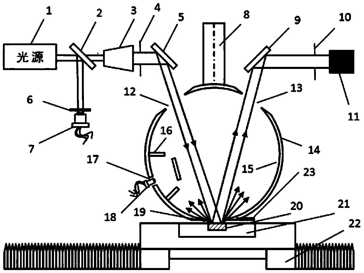
[0024] see figure 1 , an embodiment of the present invention provides a rapid surface quality detection device for planar optical elements based on total scattering measurement, which specifically includes a laser light source, a beam splitter, a laser beam expander, an aperture stop, a high reflection mirror, an integrating sphere, a CMOS Image sensor, light collector, diffuse reflector, photodetector 1, photodetector 2, XY two-dimensional guide rail, ...


PUM


Abstract

The invention relates to a plane optical component surface quality rapid detecting device and method. The device comprises a photoelectric detector 1, a photoelectric detector 2 and a two-dimensionalrotation system, wherein the photoelectric detector 1 is combined with a beam splitter and is placed in a detected light path so as to measure incident light energy; the photoelectric detector 2 is fixed in an inner detecting hole of an integrating sphere to measure scattered light energy; and the two-dimensional rotation system is used for fixing a component to be tested and is installed on an XYguide rail to achieve multi-axis linkage of the component to be tested. A measuring principle is characterized in that a detection light beam emitted by a laser light source successively passes through the beam splitter, a laser beam expander, and a high reflection mirror, and is projected into the tested component through an integrating sphere incidence hole so as to form scattered light; a mirror portion of the scattered light leaves the integrating sphere through an integrating sphere emitting / sample hole and is collected by a light collector; and a diffuse scattering portion of the scattered light is reflected multiple times in the integrating sphere to form uniform light, which is measured by the photoelectric detector 2. The detecting device can realize rapid detection of a grade ofdefects on the surface of the plane optical component.

Description

technical field [0001] The invention relates to the technical field of optical detection, in particular to a device and method for quickly detecting the surface quality of a planar optical element based on total scattering measurement. Background technique [0002] Due to the limitations of modern processing technology, optical components will inevitably leave various macroscopic defects distributed randomly on the surface after polishing, including pitting, bubbles, scratches, broken edges, broken points, etc. In precision optical systems, surface imperfections on optical components can cause light to scatter, creating background noise that degrades system performance. In addition, in high-power laser systems, surface defects can also absorb a large amount of light energy, generate thermal stress, and cause destructive effects on the normal operation of optical components and even the entire optical system. For the detection of surface defects of planar optical components,...

Claims


Application Information

Patent Timeline
Patent Type & Authority Applications(China)
IPC IPC(8): G01N21/95G01N21/958G01N21/47G01N21/01
CPCG01N21/95G01N21/958G01N21/4738G01N21/474G01N21/01G01N2021/9511G01N2021/9583G01N2021/0112
Inventor 张彬钟哲强张科鹏黄聪张小民
Owner SICHUAN UNIV
Why Eureka
Try Eureka