
A trench type silicon carbide mosfet device and its preparation method

A silicon carbide, trench technology, used in semiconductor/solid-state device manufacturing, semiconductor devices, electric solid-state devices, etc. Effects of current density, reduced on-resistance, parasitic inductance and system losses

Active Publication Date: 2020-12-18
HANGZHOU SILICON-MAGIC SEMICON TECH CO LTD
View PDF6 Cites 0 Cited by
  • Summary
  • Abstract
  • Description
  • Claims
  • Application Information

AI Technical Summary

Problems solved by technology

Although the design and optimization of full silicon carbide modules, that is, several silicon carbide MOSFETs and their antiparallel silicon carbide diodes to achieve different functions, has made great progress in recent years, but because a power switch always needs to be connected in reverse parallel with a diode, the external The diode itself will introduce additional parasitic capacitance, and at the same time, the bonding wires connected to it will introduce stray inductance, which makes the high frequency and miniaturization of silicon carbide modules always restricted
Therefore, in the past one or two years, top companies in this field, represented by General Electric of the United States and Rohm of Japan, hope to make full use of the performance of the third quadrant of SiC MOSFETs, use synchronous rectification technology, abandon anti-parallel diodes, and use integrated Schottky diodes , because the barrier height of the Schottky contact is lower than that of the Ohmic contact, it can effectively reduce the turn-on voltage, but its process requires an additional Schottky metal contact process, which is different from the existing SiC MOSFET process. compatible

Method used

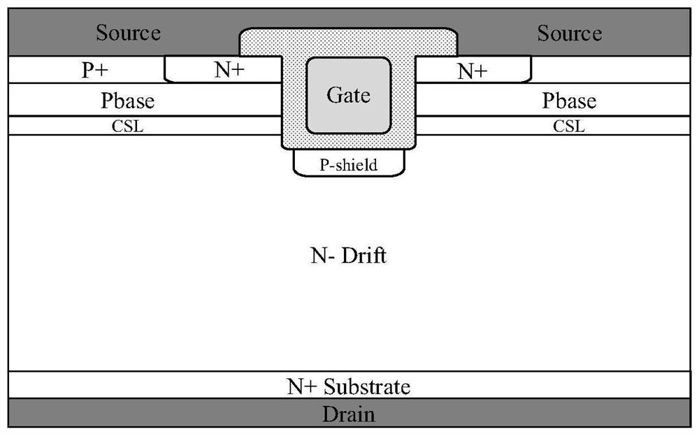
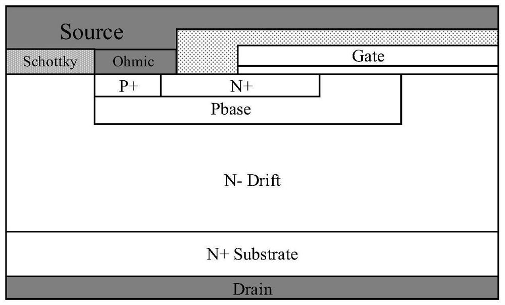

Image

  • A trench type silicon carbide mosfet device and its preparation method
  • A trench type silicon carbide mosfet device and its preparation method
  • A trench type silicon carbide mosfet device and its preparation method

Examples


Embodiment Construction

[0028] Embodiments of the present invention are described below through specific examples, and those skilled in the art can easily understand other advantages and effects of the present invention from the content disclosed in this specification. The present invention can also be implemented or applied through other different specific implementation modes, and various modifications or changes can be made to the details in this specification based on different viewpoints and applications without departing from the spirit of the present invention.

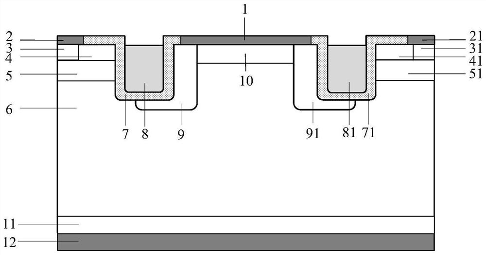
[0029] like image 3As shown, a trench silicon carbide MOSFET device includes: a drain metal 12, an N+ substrate 11 above the drain metal 12, an N-drift region 6 above the N+ substrate 11; the N-drift region 6 An N+ ohmic contact region 10 is provided in the middle of the interior of the upper part; the first P+ region 9 is provided on the left side of the N+ ohmic contact region 10, and the second P+ region 91 is provided on the righ...


PUM


Abstract

The present invention provides a trench silicon carbide MOSFET device and a preparation method thereof. The device comprises a source ohmic contact region, a drain ohmic contact region, a silicon carbide N+ substrate, a silicon carbide N drift region, a Pbase region, and an N+ source region , P+ source region, gate trench region, the invention integrates diodes inside the silicon carbide trench MOSFET device, avoids the introduction of external diodes, reduces the cell size, significantly increases the current density, reduces the on-resistance, and the device works in the third image When the time is limited, the source is positively pressed, the depletion layer of the P+ region and the N-drift region is reduced, and the N+ ohmic contact region, N ‑ The drift region, the current path from the silicon carbide N+ substrate to the ohmic contact of the drain realizes low-voltage turn-on, and the device of this invention not only maintains the characteristics of low on-resistance and high blocking voltage, but also improves the third-quadrant performance of the device , reducing device parasitic inductance and system loss, and further improving power density.

Description

technical field [0001] The invention belongs to the technical field of power semiconductors, and in particular relates to a trench type silicon carbide MOSFET device structure of an integrated diode. Background technique [0002] Silicon carbide (Silicon Carbide) material, as one of the representatives of the third-generation wide bandgap semiconductor materials, has the characteristics of large bandgap width, high critical breakdown electric field, high thermal conductivity and high electron saturation drift velocity, making it suitable for high-power , high temperature and high frequency power electronics has broad application prospects. [0003] The development of silicon carbide power MOSFET device structure is from LDMOS (lateral planar double-diffused MOSFET), VVMOS (V-groove MOSFET) to planar VDMOS (vertical double-diffused MOSFET), and then to trench MOSFET (Trench MOSFET). The structure of LDMOS is simple, but the diffusion region and the channel region are on the ...

Claims


Application Information

Patent Timeline
Patent Type & Authority Patents(China)
IPC IPC(8): H01L29/06H01L29/10H01L29/78H01L27/06H01L21/336H01L21/82
Inventor 邓小川高蜀峰柏松杨丽萍李轩张波
Owner HANGZHOU SILICON-MAGIC SEMICON TECH CO LTD
Learn More