
SiC MOSFET device with good third quadrant performance

A device and quadrant technology, applied in the direction of semiconductor devices, electrical components, circuits, etc., can solve the problem of large leakage current in the blocking state, achieve the effects of improving short-circuit capability, suppressing excessive electric field, and improving electrical characteristics and reliability

Inactive Publication Date: 2019-01-18
UNIV OF ELECTRONICS SCI & TECH OF CHINA
View PDF7 Cites 2 Cited by
  • Summary
  • Abstract
  • Description
  • Claims
  • Application Information

AI Technical Summary

Problems solved by technology

[0007] In order to optimize the performance of the third quadrant of SiC MOSFET devices and avoid bipolar degradation, and at the same time avoid the problem of excessive leakage current in the blocking state caused by the integration of the integrated Schottky interface electric field, the present invention proposes an integrated Schottky at the bottom of the groove. Diode-based SiC MOSFET devices

Method used


Image

  • SiC MOSFET device with good third quadrant performance
  • SiC MOSFET device with good third quadrant performance
  • SiC MOSFET device with good third quadrant performance

Examples


Embodiment 1

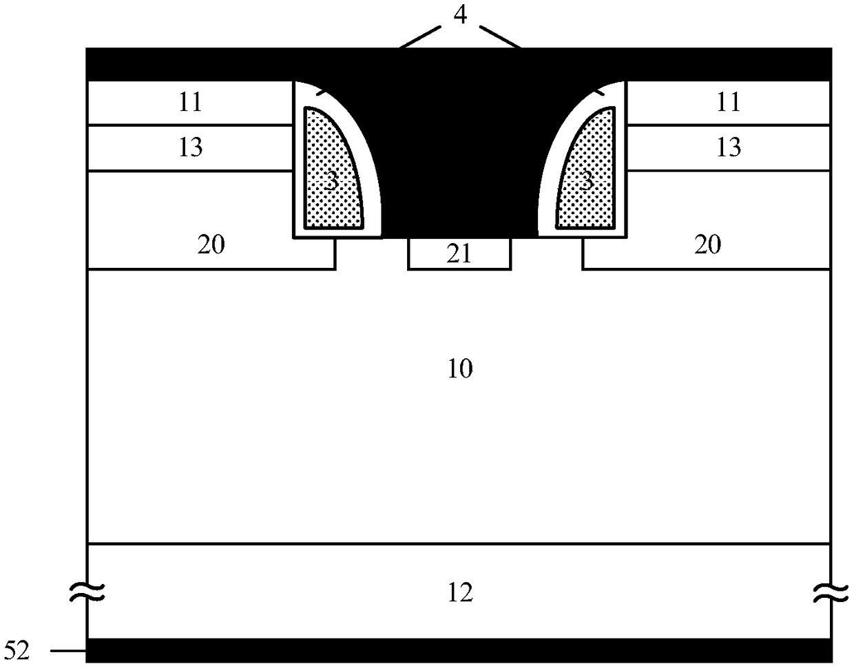
[0026] Such as figure 2 As shown, the SiC MOSFET device with good performance in the third quadrant of this embodiment includes: an N-type substrate 12, an N-type epitaxial layer 10 located above the N-type substrate 12, and a P- The body region 20, the N-type accumulation layer 13 located above the P-body region 20, the N+ contact region 11 located above the N-type accumulation layer 13, the oxide layer 4 and the side gate 3 located between the P-body regions 20, the The metal electrode 51 above the device, the drain 52 located below the device and forming ohmic contact with the N-type substrate 12, wherein the side gate 3 is connected to the N+ contact region 11, the N-type accumulation layer 13, the P-body region 20, and the metal electrode 51. The oxide layer 4 is filled between the N-type epitaxial layers 10, and the P-body region 20 wraps the lower part of the side gate 3, and the upper end of the side gate 3 is above the N-type accumulation layer 13; the metal electrod...

Embodiment 2

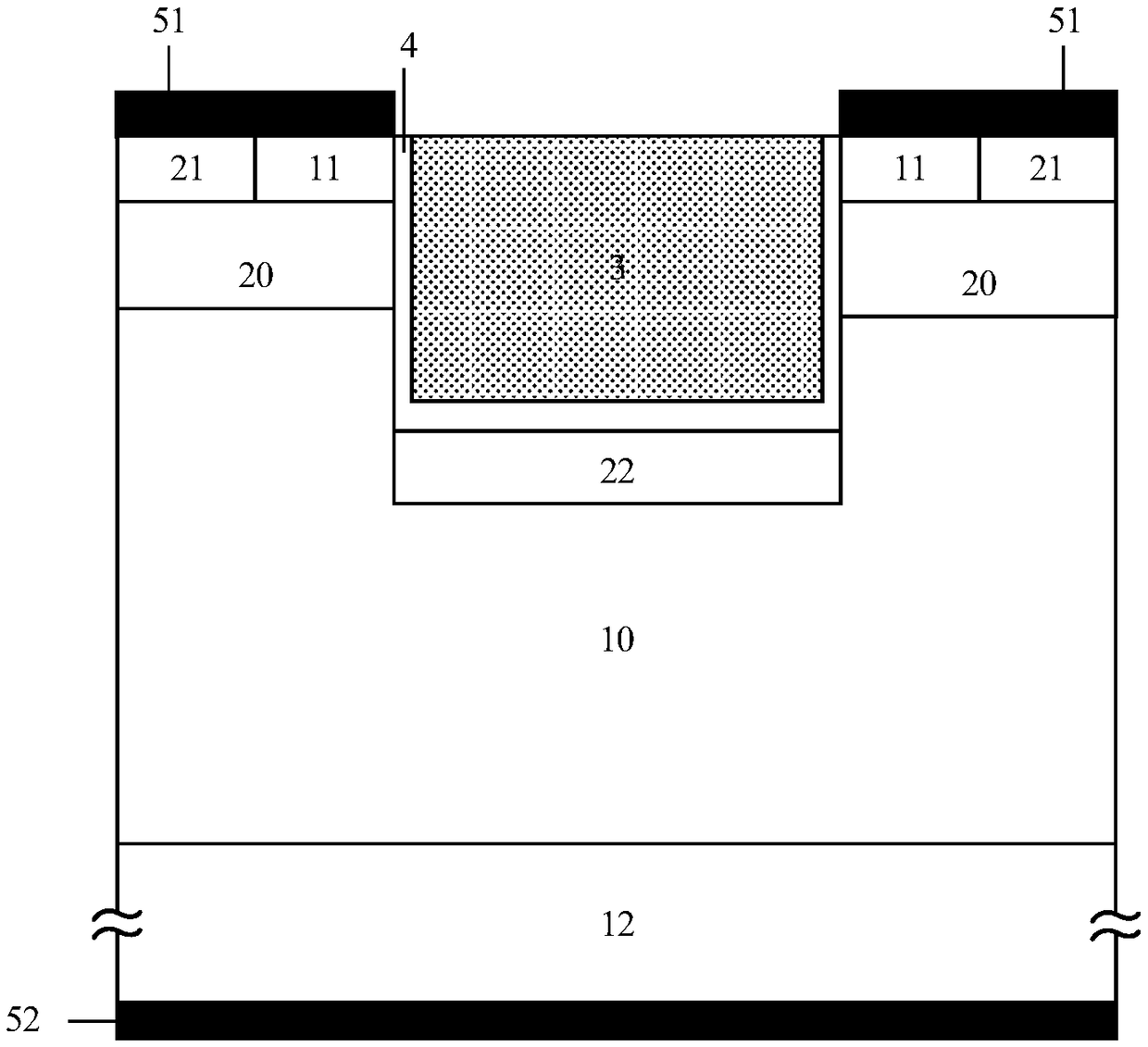
[0032] Such as image 3As shown, the difference between the device structure of this embodiment and Embodiment 1 is that a P-shield region 21 is provided under the side gate 3, and the P-shield region 21 is separated from the P-body region 20, and the P-shield region 21 is separated from the P-body region 20. The side gate 3 and the oxide layer 4 are separated.

Embodiment 3

[0034] Such as Figure 4 As shown, the main difference between this embodiment and Embodiment 2 is that the P-shield region 22 at the bottom of the groove is a plurality of separate sub-regions.


PUM


Abstract

The invention provides a SiC MOSFET device with good third quadrant performance, comprising an N-type substrate, an N-type epitaxial layer, a P- Body region, an N-type accumulation layer, an N + contact region, an oxide layer, a side gate, a metal electrode and a drain electrode. That SiC MOSFET device provide by the invention can improve the performance of the third quadrant of the SiC MOSFET, realize low reverse turn-on voltage and conduction loss, and avoid the problem of bipolar degradation. When the device is turned off, P-Body region can not only shield the electric field at the chamferof groove gate, but also protect the Schottky interface at the bottom of groove, which can effectively restrain the phenomena of excessive electric field at these two places, and improve the overall electrical characteristics and reliability of the device, the introduction of N-type accumulation layer and JFET pinch-off between the P-body regions effectively improves the short-circuiting capability of the device.

Description

technical field [0001] The invention belongs to the field of electronic science and technology, and mainly relates to power semiconductor device technology, in particular to a SiC MOSFET device with good third-quadrant performance. Background technique [0002] The wide bandgap semiconductor material SiC is an ideal material for preparing high-voltage power electronic devices. Compared with Si materials, SiC materials have a high breakdown electric field strength (4×10 6 V / cm), high carrier saturation drift velocity (2×10 7 cm / s), high thermal conductivity (490W / Mk), good thermal stability, etc., so it is especially suitable for high-power, high-voltage, high-temperature and radiation-resistant electronic devices. [0003] MOSFET is the most widely used device structure in SiC power devices. Compared with bipolar devices, SiC MOSFET has lower switching loss and higher frequency characteristics because it has no charge storage effect. [0004] Due to the poor interface stat...

Claims


Application Information

Patent Timeline
Patent Type & Authority Applications(China)
IPC IPC(8): H01L29/78H01L29/423H01L29/06
CPCH01L29/0634H01L29/4236H01L29/7813
Inventor 李轩肖家木邓小川张波
Owner UNIV OF ELECTRONICS SCI & TECH OF CHINA
Learn More