Infrared Focal Plane Array

An infrared focal plane and array technology, applied in the field of infrared focal plane arrays, can solve the problems of uneven images of focal plane arrays, different power supply voltages, etc.

Active Publication Date: 2021-07-06
WUHAN GUIDE INFRARED CO LTD
View PDF5 Cites 0 Cited by
  • Summary
  • Abstract
  • Description
  • Claims
  • Application Information

AI Technical Summary

Problems solved by technology

[0005] In view of the above defects or improvement needs of the prior art, the present invention provides an infrared focal plane array, the purpose of which is to solve the unevenness of the focal plane array image caused by the different power supply voltages between the pixels on the edge of the infrared focal plane array and the intermediate pixels. technical issues

Method used


Image

  • Infrared Focal Plane Array
  • Infrared Focal Plane Array
  • Infrared Focal Plane Array

Examples


Embodiment

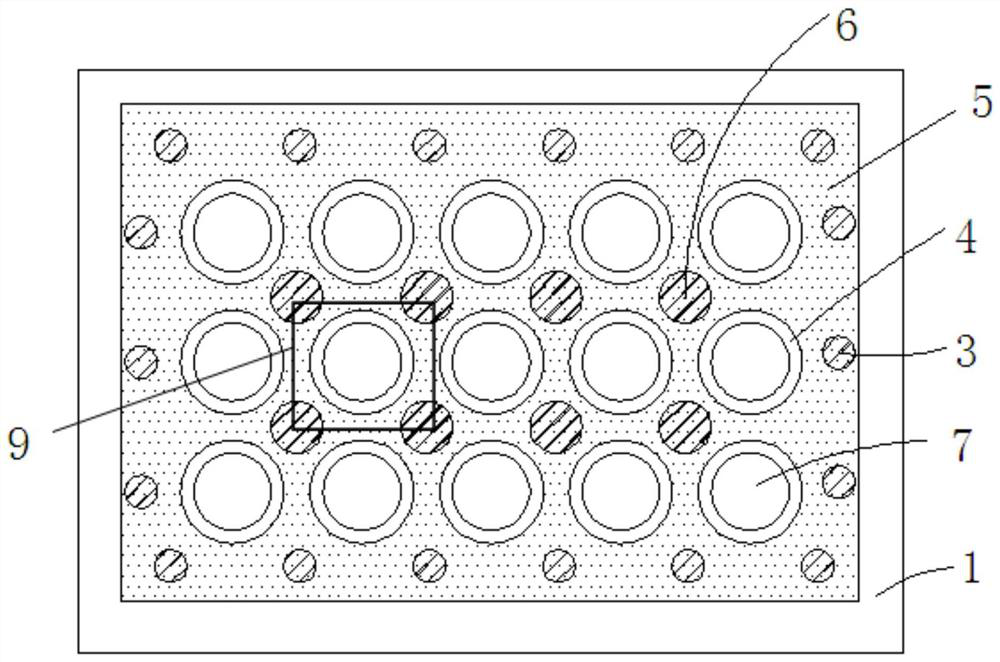
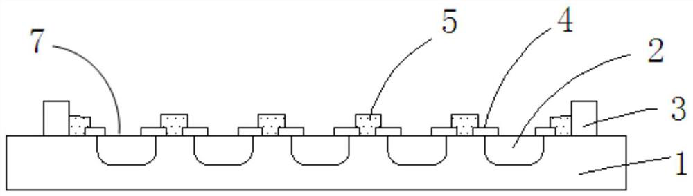
[0043] The present invention is further described below by taking the infrared focal plane array of HgCdTe material (material of epitaxial wafer) with pixels of 800×600 and pixel distance of 15 μm as an example.

[0044] In the traditional process, the current of each pixel is input by the common electrode located at the edge of the array, and then transmitted to the pixel through the HgCdTe epitaxial wafer semiconductor material. Under normal circumstances, the thickness of the epitaxial wafer material is 10-20 μm, and the resistance from the edge of the infrared focal plane array to the center of the focal plane array is more than hundreds of ohms. The working voltage should be lower than 0.12V. Since the pixel is electrically a structure containing a pn junction, the working state of the pixel is different under different operating voltages. This results in that all the pixels in the array are not in the same working state, and finally the electrical uniformity of the enti...


PUM

PropertyMeasurementUnit
thicknessaaaaaaaaaa
thicknessaaaaaaaaaa
diameteraaaaaaaaaa

Abstract

The invention discloses an infrared focal plane array, which comprises an epitaxial wafer covered with a passivation film, a plurality of sunken doping regions are arranged on the surface of the epitaxial wafer, a plurality of common electrodes are distributed on the periphery of the epitaxial wafer surface, and the passivation film is provided with A plurality of contact holes and a plurality of bump holes corresponding to a plurality of recessed doping regions; the passivation film is composed of a first passivation region and a second passivation region in the horizontal direction, and the second passivation region is A circular ring with point holes concentric to the center of the circle; the surface of the first passivation area is covered with a first conduction electrode, and the contact hole is filled with a second conduction electrode connected to the first conduction electrode; the first conduction electrode and the second The current-guiding electrodes are all made of metallic conductive materials. The purpose of the present invention is to solve the technical problem that the focal plane array picture is not uniform caused by the difference in power supply voltage between the picture elements at the edge of the infrared focal plane array and the middle picture elements.

Description

technical field [0001] The invention belongs to the field of optoelectronic technology, and more particularly, relates to an infrared focal plane array. Background technique [0002] An infrared detector is a light sensor that can respond to external infrared light radiation. A two-dimensional array composed of multiple infrared detector units is called an infrared focal plane array, which is the core of an infrared detector. Infrared detectors can be divided into photon detectors and thermal detectors according to their working mechanism. After photon detectors receive infrared radiation, they can directly convert optical signals into electrical signals. Photon detectors are characterized by high sensitivity and response. It has fast speed and high response frequency. Generally, it needs to work at low temperature and has a narrow detection band. [0003] With the development of infrared focal plane array technology, the area of ​​the focal plane array is getting larger an...

Claims


Application Information

Patent Timeline
Patent Type & Authority Patents(China)
IPC IPC(8): H01L27/144H01L31/0224H01L31/18
CPCH01L27/1443H01L27/1446H01L31/02161H01L31/022408H01L31/1832Y02P70/50
Inventor 金迎春高健飞黄立刘斌
Owner WUHAN GUIDE INFRARED CO LTD
Why Eureka
Try Eureka