High-voltage semiconductor component

A technology for semiconductors and components, applied in the field of high-voltage semiconductor components, can solve the problems of high breakdown voltage of high-voltage semiconductor components, etc., and achieve the effects of reducing surface electric field, reducing surface current, and increasing breakdown voltage

Active Publication Date: 2019-04-02
NUVOTON
View PDF32 Cites 2 Cited by
  • Summary
  • Abstract
  • Description
  • Claims
  • Application Information

AI Technical Summary

Problems solved by technology

As the size of electronic components continues to shrink, it is increasingly difficult to maintain high breakdown voltages of high-voltage semiconductor components

Method used


Image

  • High-voltage semiconductor component
  • High-voltage semiconductor component
  • High-voltage semiconductor component

Examples


Embodiment Construction

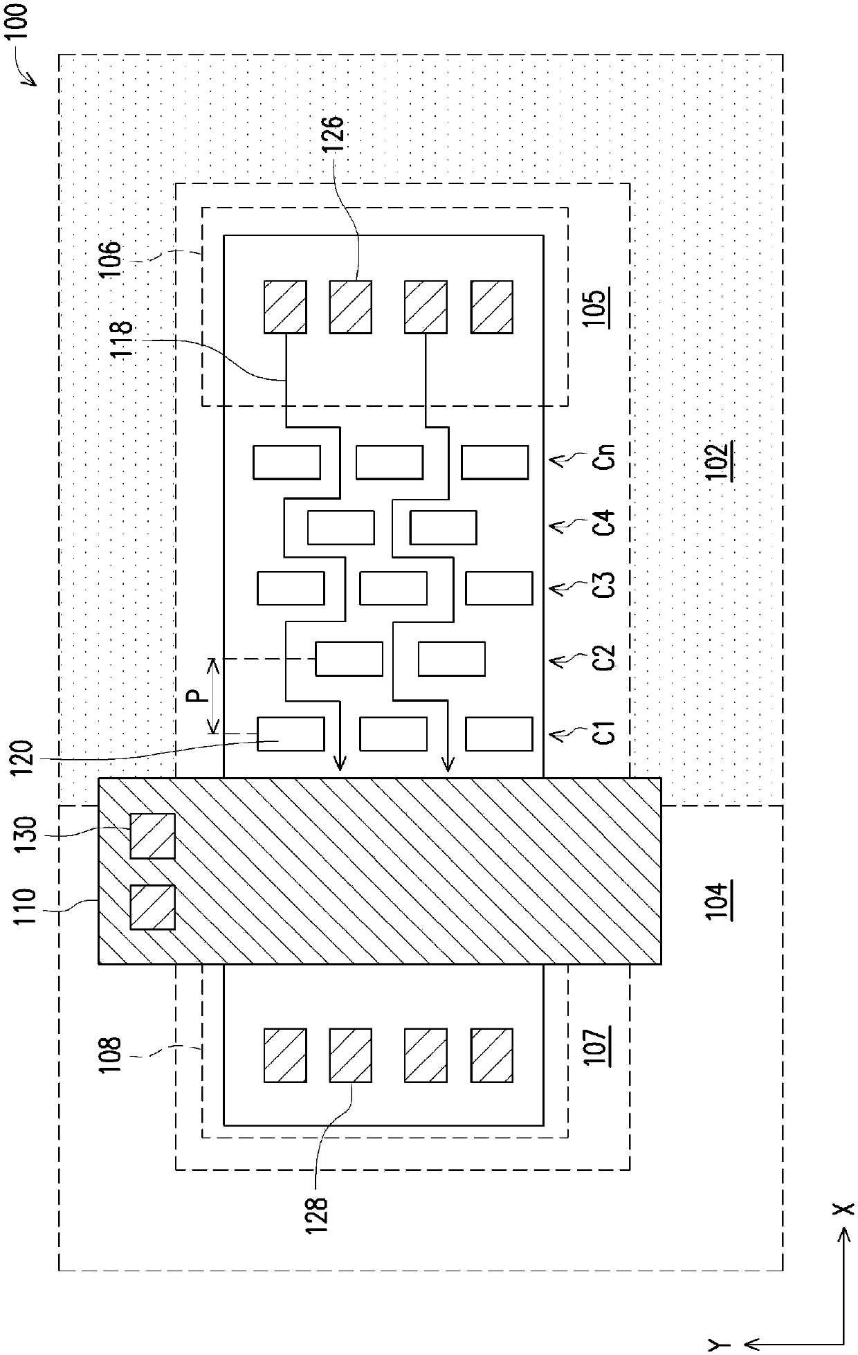
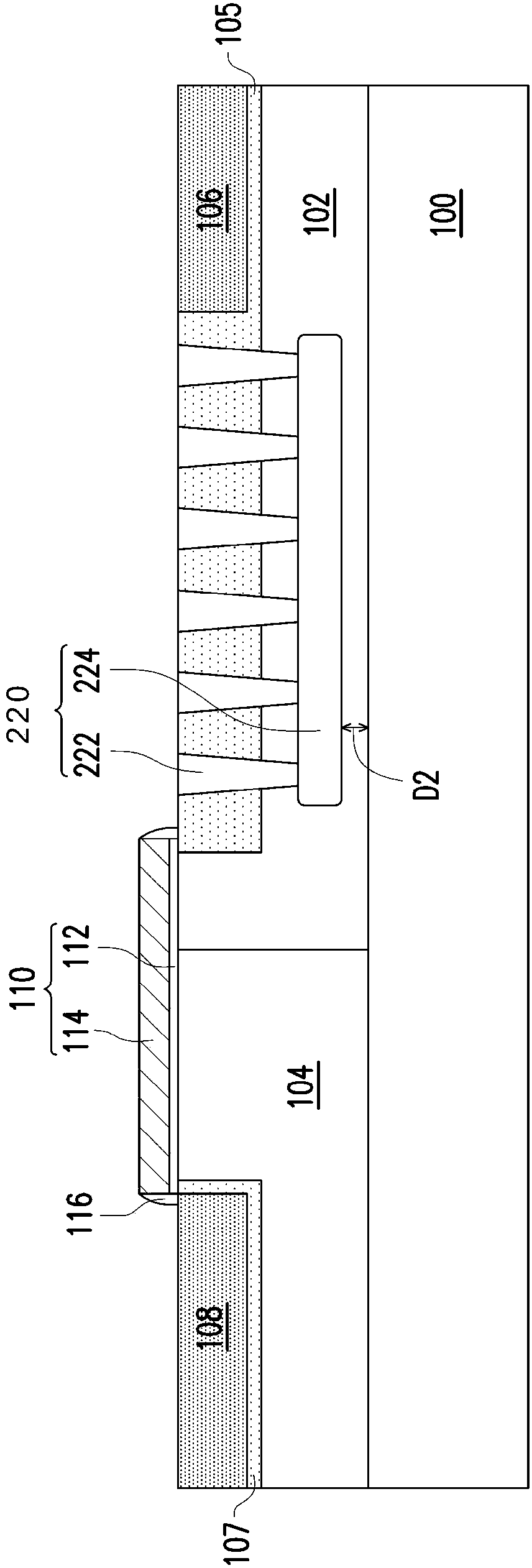
[0055] The present invention will be described more fully with reference to the drawings of the present embodiment. However, the present invention can also be embodied in various forms and should not be limited to the embodiments described herein. The thicknesses of layers and regions in the drawings may be exaggerated for clarity. The same or similar reference numerals represent the same or similar elements, and the following paragraphs will not repeat them.

[0056] In the following embodiments, when the first conductivity type is N type, the second conductivity type is P type; when the first conductivity type is P type, the second conductivity type is N type. The P-type dopant is, for example, boron; the N-type dopant, for example, is phosphorus or arsenic. In this embodiment, the first conductivity type is P-type and the second conductivity type is N-type as an example for illustration, but the present invention is not limited thereto.

[0057] figure 1 is a schematic ...


PUM


Abstract

The invention discloses a high-voltage semiconductor component comprising a substrate, a first well region having a second conductivity type, a second well region having a first conductivity type, a first doped region, a second doped region, a gate structure and multiple isolation structures. The first well region is located on the substrate. The second well region is located on the substrate nextto the first well region. The first doped region is located in the first well region. The second doped region is located in the second well region. The gate structure is loated on the substrate between the first doped region and the second doped region. The isolation structures are located in the first well region. The isolation structures are staggered in an array. Each isolation structure includes a dielectric pillar and a top doped region below the dielectric pillar. The bottom surface of the first well region is lower than the bottom surface of each isolation structure.

Description

technical field [0001] The present invention relates to a semiconductor element, and in particular to a high-voltage semiconductor element. Background technique [0002] Generally speaking, high-voltage semiconductor components are mainly used in power switching circuits. It has become a trend to intelligentize the power switching circuit to make power management techniques more efficient. In this trend, analog or digital control electronics and power transistors can be integrated on the same chip. [0003] With the advancement of science and technology, electronic components are developing towards thinner and lighter. As the size of electronic components continues to shrink, it becomes increasingly difficult to maintain high breakdown voltages of high-voltage semiconductor components. Therefore, how to increase the breakdown voltage of high-voltage semiconductor elements under a certain element size or miniaturized element size will become an important subject. Content...

Claims


Application Information

Patent Timeline
Patent Type & Authority Applications(China)
IPC IPC(8): H01L29/06H01L27/02
CPCH01L27/0207H01L29/063H01L29/0684H01L29/7835H01L29/0653H01L29/0692H01L29/0634
Inventor 韦维克陈柏安
Owner NUVOTON
Why Eureka
Try Eureka