Double-layer/multilayer thermoelectric device and preparation method thereof
A thermoelectric device, double-layer technology, used in the manufacture/processing of thermoelectric devices, junction lead-out materials of thermoelectric devices, thermoelectric devices using only the Peltier or Seebeck effect, etc.
- Summary
- Abstract
- Description
- Claims
- Application Information
AI Technical Summary
Problems solved by technology
Method used
Image
Examples
Embodiment 1
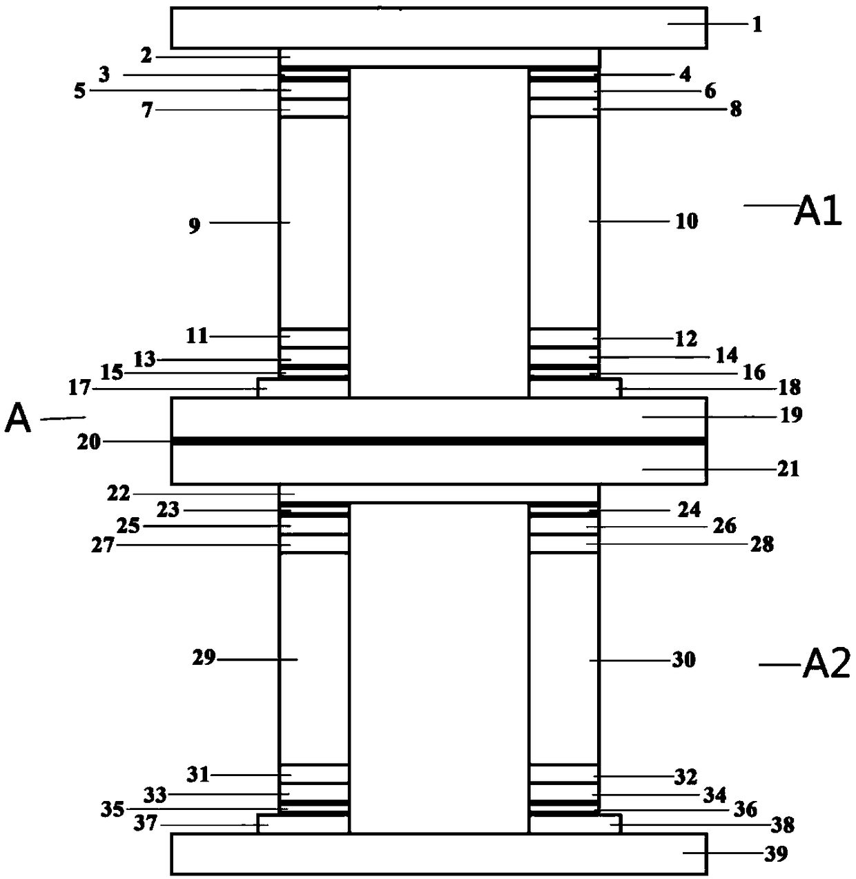
[0054] Please see figure 1 , the double-layer thermoelectric device A includes two upper and lower thermoelectric sub-modules A1 and A2 with the same structure, corresponding to the high temperature section and the low temperature section respectively. The thermoelectric sub-module contains a pair of n-type and p-type thermoelectric arms. Each set of thermoelectric arms has the following 5 layers, from top to bottom: high melting point metal layers 5 and 6, metallization layers 7 and 8, and thermoelectric materials 9 and 10 , metallization layers 11 and 12, high melting point metal layers 13 and 14; the two ends of the above-mentioned pair of thermoelectric arms 1 and 2 are connected to the pure copper conductive connecting piece 2 or On the conductive connecting sheets 17 and 18, the thickness is 0.8 mm, and further connected to the AlN high thermal conductivity ceramic sheet 1 or 19 with a thickness of 0.38 mm. Correspondingly, the thermoelectric sub-module A2 also has the ...
Embodiment 2-4
[0067] The structure of the double-layer thermoelectric device in Examples 2-4 is basically the same as that of Example 1, and its preparation method is also very similar, except that the selected thermoelectric material and the corresponding metallization layer and the type of high melting point metal are different, as shown in the following table 1 shown
[0068]
[0069] The metallization layer and high melting point metal used are shown in Table 2
[0070]
High temperature section metallization layer
Metallization layer in low temperature section
High melting point metal in high temperature section
Metals with high melting point in low temperature section
Example 2
co 0.8 Fe 0.2
Ni
Cu
Cu
Example 3
co 0.7 Fe 0.3
Ni
Cu
Cu
Example 4
co 0.6 Fe 0.4
Ni
Cu
Cu
[0071] Among them, the thickness of each layer is shown in the following table 3
[0072]
[0073] Where...
PUM
| Property | Measurement | Unit |
|---|---|---|
| thickness | aaaaa | aaaaa |
| thickness | aaaaa | aaaaa |
| thickness | aaaaa | aaaaa |
Abstract
Description
Claims
Application Information
 - Generate Ideas
- Intellectual Property
- Life Sciences
- Materials
- Tech Scout
- Unparalleled Data Quality
- Higher Quality Content
- 60% Fewer Hallucinations
Browse by: Latest US Patents, China's latest patents, Technical Efficacy Thesaurus, Application Domain, Technology Topic, Popular Technical Reports.
© 2025 PatSnap. All rights reserved.Legal|Privacy policy|Modern Slavery Act Transparency Statement|Sitemap|About US| Contact US: help@patsnap.com


