Preparation method of microstructure surface with alternate hydrophilic-hydrophobic distribution
A microstructure, hydrophilic and hydrophobic technology, applied in coatings and other directions, can solve problems affecting the ecological environment and achieve the effect of improving broad-spectrum antifouling performance
- Summary
- Abstract
- Description
- Claims
- Application Information
AI Technical Summary
Problems solved by technology
Method used
Image
Examples
Embodiment 1
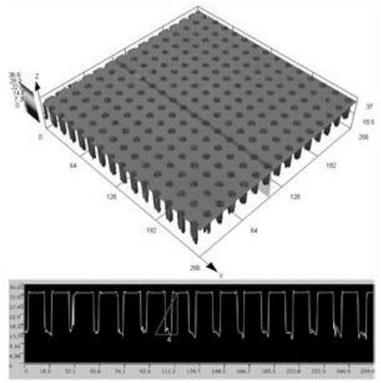
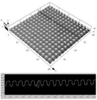
[0020] The process of the method for preparing the surface of the hydrophilic-hydrophobic interactive distribution microstructure involved in this embodiment is as follows: first, the photomask with the set pattern is etched by electron beams, and the photomask is covered on the surface of the single crystal silicon; A set pattern with a depth of 20 microns is etched on the silicon surface, and the etched single crystal silicon surface is used as a negative mold, such as figure 1 As shown, the hydrophobic silicone microstructure surface was obtained by turning over the mold, and then, under vacuum conditions, the hydrophobic silicone microstructure surface was subjected to plasma activation treatment with a voltage of 1.0V and a current of 0.4A for 10 minutes, followed by , drip hydrochloric acid hydrogen peroxide solution on the surface of the hydrophobic silicone microstructure, and cover a layer of dimethyl silicone oil, after 15 minutes, rinse the surface of the hydrophobic...
Embodiment 2
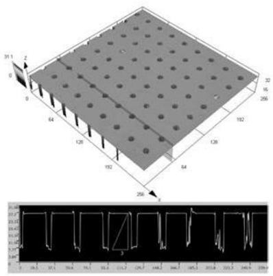
[0022] The process of the method for preparing the surface of the hydrophilic-hydrophobic interactive distribution microstructure involved in this embodiment is as follows: first, the photomask with the set pattern is etched by electron beams, and the photomask is covered on the surface of the single crystal silicon; A set pattern with a depth of 20 microns is etched on the silicon surface, and the etched single crystal silicon surface is used as a negative mold, such as image 3 As shown, the hydrophobic silicone microstructure surface was obtained by turning over the mold, and then, under vacuum conditions, the hydrophobic silicone microstructure surface was subjected to plasma activation treatment with a voltage of 3.0V and a current of 2.0A for 5 minutes, followed by , drop hydrochloric acid hydrogen peroxide solution on the surface of the hydrophobic silicone microstructure, and cover a layer of liquid paraffin, after 5 minutes, rinse the hydrophobic silicone microstructur...
Embodiment 3
[0024] The process of the method for preparing the surface of the hydrophilic-hydrophobic interactive distribution microstructure involved in this embodiment is as follows: first, the photomask with the set pattern is etched by electron beams, and the photomask is covered on the surface of the single crystal silicon; Etch a set pattern with a depth of 10 microns on the silicon surface, use the etched single crystal silicon surface as a negative mold, and obtain a hydrophobic organic silicon microstructure surface by turning over the mold, and then, under vacuum conditions, with a voltage of 2.0V and a current of 1.0A to perform plasma activation treatment on the surface of the hydrophobic organosilicon microstructure for 8 minutes. Next, drop hydrochloric acid and hydrogen peroxide solution on the surface of the hydrophobic organosilicon microstructure, and cover a layer of two layers with a volume ratio of 1:1. A mixed liquid of methyl silicone oil and methyl phenyl silicone o...
PUM
 Abstract
Description
Claims
Application Information
 - R&D
- Intellectual Property
- Life Sciences
- Materials
- Tech Scout
- Unparalleled Data Quality
- Higher Quality Content
- 60% Fewer Hallucinations
Browse by: Latest US Patents, China's latest patents, Technical Efficacy Thesaurus, Application Domain, Technology Topic, Popular Technical Reports.
© 2025 PatSnap. All rights reserved.Legal|Privacy policy|Modern Slavery Act Transparency Statement|Sitemap|About US| Contact US: help@patsnap.com


