LED chip with annular electrode structure and method for preparing LED chip

A technology of LED chips and ring electrodes, applied in the field of optoelectronics, can solve the problem of limited improvement in brightness, and achieve the effects of improving brightness, reducing etching area, and making wire bonding easier

Inactive Publication Date: 2019-02-12
SHANDONG INSPUR HUAGUANG OPTOELECTRONICS
View PDF6 Cites 4 Cited by
  • Summary
  • Abstract
  • Description
  • Claims
  • Application Information

AI Technical Summary

Problems solved by technology

Although this method improves the luminous efficiency by turning the finger line into a discontinuous electrode through hole, the improvement of the brightness is limited, and there is still the problem of the height difference between the P electrode and the N electrode.

Method used


Image

  • LED chip with annular electrode structure and method for preparing LED chip
  • LED chip with annular electrode structure and method for preparing LED chip
  • LED chip with annular electrode structure and method for preparing LED chip

Examples


Embodiment Construction

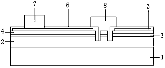
[0026] different from figure 1 The conventional LED chip shown, the LED chip with ring electrode structure of the present invention, as figure 2 As shown, it includes a substrate 1 , an n-type GaN layer 2 , a quantum well layer 3 and a p-type GaN layer 4 sequentially arranged from bottom to top. An annular mesa is arranged on the n-type GaN layer 2 , a transparent conductive layer 5 is arranged on the p-type GaN layer 4 , and a passivation layer 6 is arranged on the transparent conductive layer 5 . A p-electrode 7 is arranged on the transparent conductive layer 5, and an n-electrode 8 is arranged on the ring-shaped mesa, and the n-electrode 8 is ring-shaped.

[0027] The substrate 1 may be a sapphire substrate, a SiC substrate or a silicon substrate. The transparent conductive layer 5 is ITO (indium tin oxide), ZnO or graphene. Passivation layer 6 is SiO 2 or SiN. The p-electrodes 7 and n-electrodes 8 are composed of two or more metal film systems of Cr, Ti, Pd, Pt, Al, ...


PUM


Abstract

The invention discloses an LED chip with an annular electrode structure and a method for preparing the LED chip. The LED chip is characterized in that a transparent conducting layer is arranged on a p-type GaN layer, a passivation layer is arranged on the transparent conducting layer, an annular tabletop is arranged on an n-type GaN layer, a p electrode is arranged on the transparent conducting layer, and an annular n electrode is arranged on the annular tabletop. The method for preparing the LED chip includes steps of (1), acquiring GaN-based epitaxial slices; (2), etching the annular tabletop by the aid of masks with annular structures; (3), forming the transparent conducting layer; (4), manufacturing the passivation layer; (5), corroding the passivation layer; (6), preparing the p electrode on the passivation layer on a surface of the p-type GaN layer and preparing the n electrode on the annular tabletop. The LED chip and the method have the advantages that the LED chip is providedwith the annular electrode structure, accordingly, the problem of height difference of existing p and n electrodes can be solved, wires are easy to weld, and the etching areas of active layers can bereduced; reflection effects can be realized by the metal electrodes, accordingly, light around the electrodes can be reflected, and the brightness can be improved.

Description

technical field [0001] The invention relates to an LED (light-emitting diode) chip and a preparation method thereof, in particular to an electrode structure of the LED chip, and belongs to the field of optoelectronic technology. Background technique [0002] As one of the most valued light source technologies, on the one hand, LED has the characteristics of small size; on the other hand, it has the power saving characteristics of low current and low voltage drive; Longevity and many other advantages. Among them, as one of the main applications in the field of optoelectronics, GaN-based materials have attracted more and more attention. GaN-based semiconductor materials can be used to produce ultra-high brightness blue, green, and white light-emitting diodes. Nowadays, downstream applications have higher and higher requirements on the brightness of LED chips, so various technologies to improve the brightness of LEDs have emerged, such as patterned substrate technology, sidewa...

Claims


Application Information

Patent Timeline
Patent Type & Authority Applications(China)
IPC IPC(8): H01L33/38
CPCH01L33/38H01L2933/0016
Inventor 吴向龙闫宝华彭璐刘琦肖成峰
Owner SHANDONG INSPUR HUAGUANG OPTOELECTRONICS
Why Eureka
Try Eureka