Backside-illuminated CMOS sensor and manufacturing method thereof

A technology of a CMOS sensor and a manufacturing method, which is applied to radiation control devices and other directions, can solve problems such as lack of records, and achieve the effects of reducing etching area, improving imaging quality, and increasing effective circuit area

Active Publication Date: 2015-04-29
OMNIVISION TECH (SHANGHAI) CO LTD
View PDF5 Cites 0 Cited by
  • Summary
  • Abstract
  • Description
  • Claims
  • Application Information

AI Technical Summary

Problems solved by technology

This patent document does not describe how to increase the effective area of ​​the back-illuminated CMOS sensor without increasing the area of ​​the CMOS sensor

Method used


Image

  • Backside-illuminated CMOS sensor and manufacturing method thereof
  • Backside-illuminated CMOS sensor and manufacturing method thereof
  • Backside-illuminated CMOS sensor and manufacturing method thereof

Examples


preparation example Construction

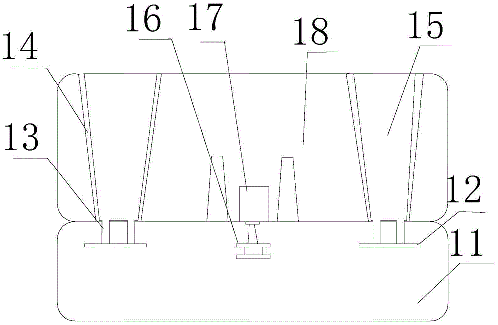
[0031] In the actual preparation process, if the area is 4127um×4127um=1.7E8um 2 The newly increased effective area of ​​the COMS sensor can reach 55um×110um×26×4=6.3E6um 2 , thereby increasing the area of ​​the adjustable device structure region by 6.3E6 / 1.7E8×100%≈3.7%, which greatly increases the effective area of ​​the adjustable device structure of the CMOS sensor.

[0032] Preferably, an isolation structure such as a shallow trench isolation structure (STI), etc. is also provided around the above-mentioned newly added device structure 17 .

[0033] Further, a plurality of connecting wire structures are arranged in the dielectric layer 11 corresponding to the above-mentioned device layer 18, that is, a metal layer 12 is arranged at a position corresponding to each connecting pad 15, and the metal layer 12 is connected to the connecting wire 13 through the connecting wire 13. The disk 15 is connected; at the position corresponding to the above-mentioned newly added device...


PUM


Abstract

The invention relates to the field of semiconductor manufacturing, in particular to a backside-illuminated CMOS sensor and a manufacturing method thereof. By changing design of an etching pattern of wafer backside silicon, the etching area is reduced, namely in a dry etching process, only a device layer in a groove of a connecting plate is removed, so that a new circuit structure can be added, and thus an effective circuit area is increased on the premise of not increasing the area of the sensor. Through the area, during facade design of a wafer, some circuits can be additionally arranged so as to improve the imaging quality of the CMOS sensor.

Description

technical field [0001] The invention relates to the field of semiconductor manufacturing, in particular to a back-illuminated CMOS sensor and a manufacturing method thereof. Background technique [0002] The back-illuminated CMOS sensor (BSI CMOS sensor) turns the direction of the original photosensitive layer so that the light enters directly from the back of the device, thus effectively avoiding the traditional CMOS sensor structure, where the light needs to pass between the microlens and the photodiode. Only the circuit, transistor and other structural layers can reach the photosensitive layer, which significantly improves the light efficiency and greatly improves the photosensitive effect under low light conditions. [0003] With the development of technology, people's requirements for user experience are getting higher and higher, so the requirements for imaging quality of back-illuminated CMOS sensors are also getting higher and higher. However, under the premise of c...

Claims


Application Information

Patent Timeline
Patent Type & Authority Applications(China)
IPC IPC(8): H01L27/146
Inventor 高喜峰费孝爱
Owner OMNIVISION TECH (SHANGHAI) CO LTD
Why Eureka
Try Eureka