Silicon carbide pressure sensor chip with multi-layer relief and island film structure and preparation method thereof

A pressure sensor, silicon carbide technology, applied in the direction of fluid pressure measurement by changing ohmic resistance, microstructure technology, measurement of fluid pressure, etc., can solve the problem that the pressure sensor chip is difficult to achieve series-parallel resistance temperature compensation, silicon carbide pressure sensor manufacturing efficiency Low sensor linearity and other problems, to increase the anti-overload capability, reduce nonlinearity, reduce the effect of center deflection

Active Publication Date: 2022-08-05
XI AN JIAOTONG UNIV
View PDF9 Cites 0 Cited by
  • Summary
  • Abstract
  • Description
  • Claims
  • Application Information

AI Technical Summary

Problems solved by technology

[0006] The purpose of the present invention is to overcome the shortcomings of the above-mentioned prior art, and provide a silicon carbide pressure sensor chip with a multi-layer relief and island film structure and its preparation method, so as to solve the problem of large-area engraving in the preparation process of the silicon carbide sensor chip in the prior art. The corrosion efficiency is low, the manufacturing efficiency of silicon carbide pressure sensor is low, the linearity of the prepared sensor is easy to decrease with the increase of working temperature, and the technical problem that the pressure sensor chip is difficult to realize the temperature compensation of series and parallel resistance in high temperature environment

Method used


Image

  • Silicon carbide pressure sensor chip with multi-layer relief and island film structure and preparation method thereof
  • Silicon carbide pressure sensor chip with multi-layer relief and island film structure and preparation method thereof
  • Silicon carbide pressure sensor chip with multi-layer relief and island film structure and preparation method thereof

Examples


Embodiment Construction

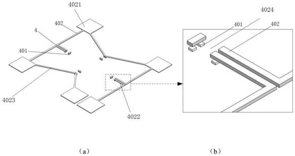
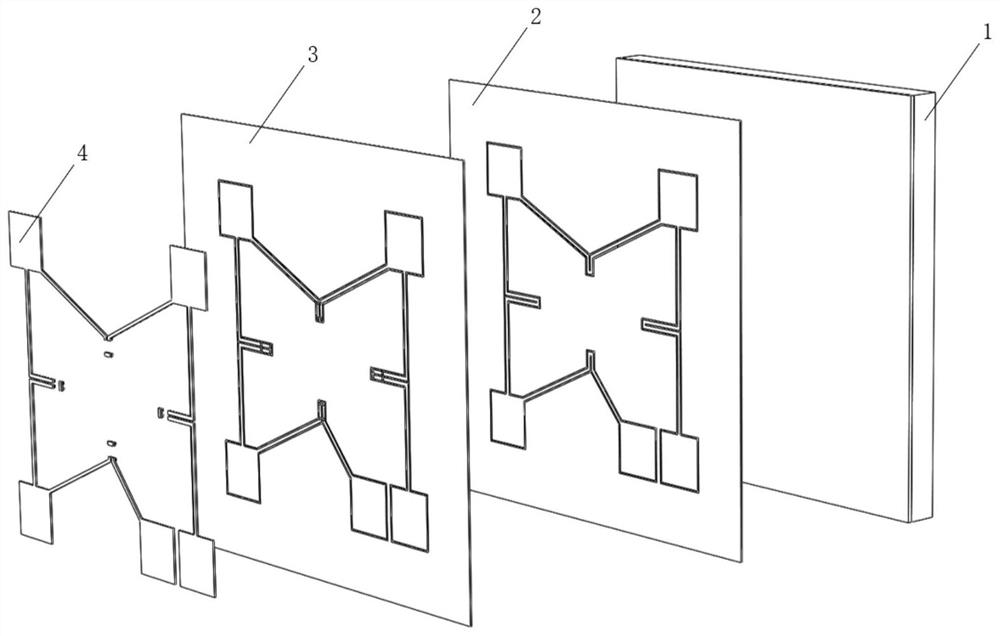
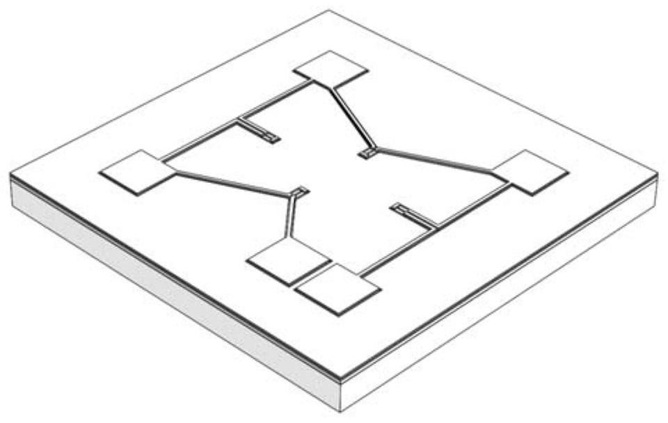
[0051] Below in conjunction with accompanying drawing, the present invention is described in further detail:

[0052] In the description of the present invention, it should be noted that the terms "center", "upper", "lower", "left", "right", "vertical", "horizontal", "inner", "outer", etc. The indicated orientation or positional relationship is based on the orientation or positional relationship shown in the accompanying drawings, which is only for the convenience of describing the present invention and simplifying the description, rather than indicating or implying that the indicated device or element must have a specific orientation or a specific orientation. construction and operation, and therefore should not be construed as limiting the invention; the terms "first", "second", "third" are used for descriptive purposes only and should not be construed as indicating or implying relative importance; furthermore, unless otherwise Clearly stipulated and defined, the terms "inst...


PUM

PropertyMeasurementUnit
thicknessaaaaaaaaaa
thicknessaaaaaaaaaa
thicknessaaaaaaaaaa

Abstract

The invention discloses a silicon carbide pressure sensor chip with a multi-layer relief and island film structure and a preparation method thereof. The chip structure includes a chip substrate, a silicon carbide relief layer, an insulating relief layer and a metal relief layer sequentially stacked from bottom to top. ; The silicon carbide relief layer is separated from the silicon carbide bridge road relief layer and the silicon carbide outer frame relief layer and the silicon carbide inner frame relief layer by setting a narrow isolation channel, and the structures of the insulating relief layer and the metal relief layer are both. Relying on the silicon carbide relief layer, the structure of the insulating relief layer is the same as that of the silicon carbide relief layer, and the structure of the metal relief layer is the same as that of the silicon carbide bridge relief layer. The insulating relief layer isolates the silicon carbide relief layer and the metal relief layer in all areas except the contact port, so that the electrical signal can be conducted in the designated contact port, and then realizes the bridge with the silicon carbide through the contact point metal layer. The electrical connection of the road relief layer.

Description

technical field [0001] The invention belongs to the technical field of micro-electromechanical system (MEMS) pressure sensor manufacturing, and in particular relates to a silicon carbide pressure sensor chip with a multi-layer relief and island film structure and a preparation method thereof. Background technique [0002] As an important product of micro-electromechanical systems (MEMS), high temperature pressure sensors have broad application requirements in the fields of civil industry and national defense and military industries. At present, the commercialized MEMS pressure sensors are mainly silicon diffusion piezoresistive pressure sensors, which have mature technology and excellent performance, but are limited by the temperature resistance of the PN junction. When the temperature exceeds 120 °C, the performance of the sensor will seriously deteriorate or even fail. At 500°C, the silicon diffusion sensor chip will have plastic deformation and current leakage, which cann...

Claims


Application Information

Patent Timeline
Patent Type & Authority Patents(China)
IPC IPC(8): G01L1/18G01L9/06B81B7/02B81C1/00
CPCG01L1/18G01L9/06G01L9/065B81B7/02B81C1/00436B81B2201/0264
Inventor 赵玉龙王鲁康赵友杨玉
Owner XI AN JIAOTONG UNIV
Why Eureka
Try Eureka