A hybrid anode diode with nano-fin gate structure
A hybrid anode and diode technology, applied in the direction of semiconductor devices, electrical components, circuits, etc., can solve the problems of high reverse withstand voltage, increase the forward working loss of devices, low forward turn-on voltage, etc., achieve high withstand voltage, reduce Effects of material damage and low turn-on voltage
Active Publication Date: 2021-02-12
HANGZHOU SILICON-MAGIC SEMICON TECH CO LTD
View PDF7 Cites 0 Cited by
- Summary
- Abstract
- Description
- Claims
- Application Information
AI Technical Summary
Problems solved by technology
Larger turn-on voltage will increase the forward operating loss of the device, so developing a high-performance GaN power diode with low forward turn-on voltage and high reverse withstand voltage is of great significance for practical applications
Method used
View moreImage
Smart ImageViewing Examples

Examples
Embodiment Construction
[0020] The present invention has been described in detail in the part of the summary of the invention, and will not be repeated here.
Login to View More PUM
 Abstract
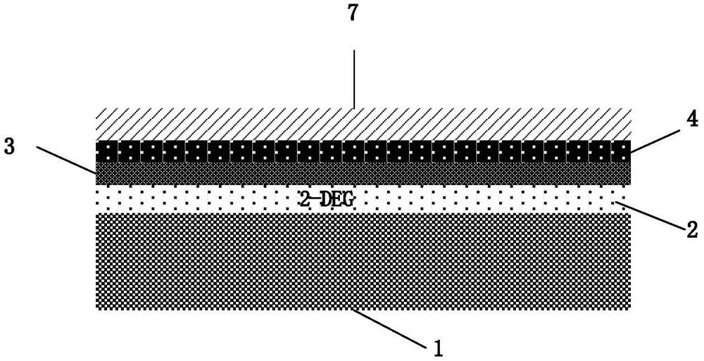
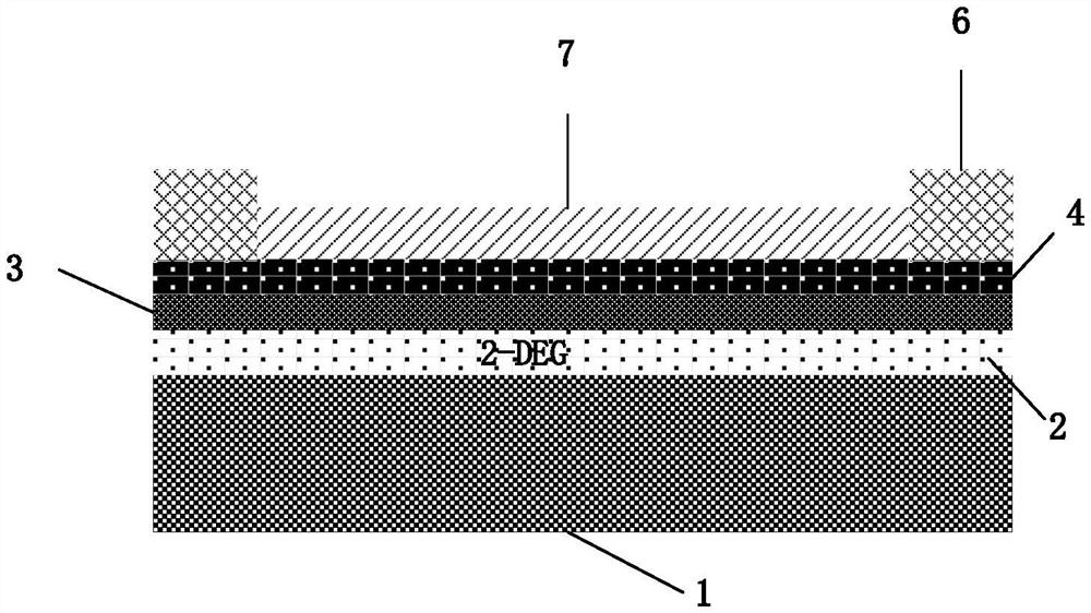
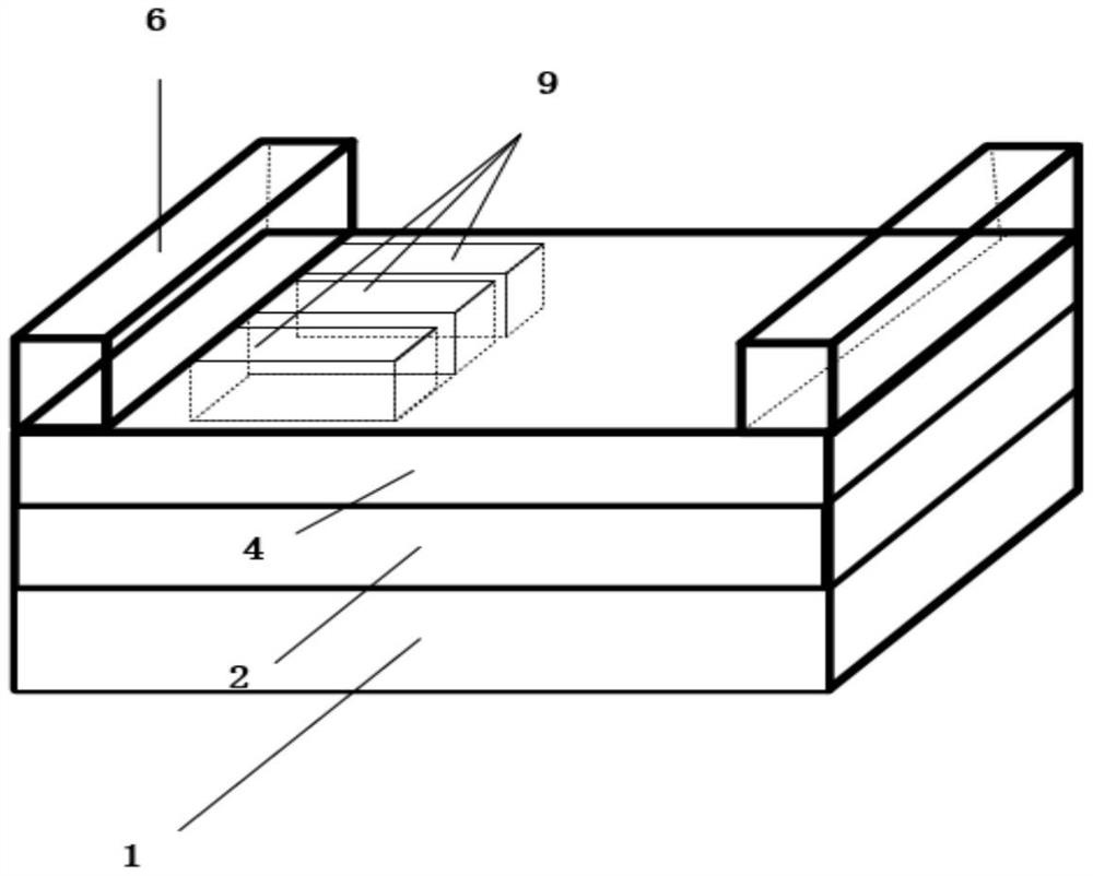
The invention belongs to the technical field of semiconductors and relates to a mixed anode diode with a Nano-Fin gate structure. In the present invention, the gate is a Nano-Fin structure, and the barrier layer is etched into a finger shape by equal or unequal spacing, so that the two-dimensional electron gas concentration in the heterojunction under the gate groove and between the gate grooves can be adjusted. A new technique of modulation. Beneficial effects of the present invention: the purpose of partially depleting the two-dimensional electron gas under the gate to realize an enhanced channel is realized. In the process, such as annealing, the impact of high temperature processes such as gate dielectric growth process on the distribution of implanted ions; device characteristics such as turn-on voltage, on-resistance, and reverse leakage of the diode of the present invention can be changed by changing the number of FIN-shaped structures and the FIN-shaped structure. The width of the structure is adjusted.
Description
technical field [0001] The invention belongs to the technical field of power semiconductors and relates to a mixed anode diode with a Nano-Fin gate structure. Background technique [0002] Gallium Nitride (GaN) is a third-generation wide-bandgap semiconductor material. It has stable chemical properties, high temperature resistance, and corrosion resistance. It is very suitable for making radiation-resistant, high-frequency, high-power, and high-density integrated electronic devices. All these excellent properties make up for the inherent shortcomings of the previous two generations of semiconductor materials such as Si and GaAs, thus becoming a rapidly developing research frontier. [0003] As the third-generation wide-bandgap semiconductor device, GaN-based Schottky barrier diode (SBD) power device has excellent characteristics such as high temperature resistance, high voltage resistance and small on-resistance, and has significant advantages in power devices. The traditio...
Claims
Login to View More Application Information
Patent Timeline
 Patent Type & Authority Patents(China)
IPC IPC(8): H01L29/778H01L29/423
CPCH01L29/42316H01L29/7787
Inventor 周琦胡凯张安邦朱厉阳张波
Owner HANGZHOU SILICON-MAGIC SEMICON TECH CO LTD
Features
- R&D
- Intellectual Property
- Life Sciences
- Materials
- Tech Scout
- Unparalleled Data Quality
- Higher Quality Content
- 60% Fewer Hallucinations
Learn More Browse by: Latest US Patents, China's latest patents, Technical Efficacy Thesaurus, Application Domain, Technology Topic, Popular Technical Reports.
© 2025 PatSnap. All rights reserved.Legal|Privacy policy|Modern Slavery Act Transparency Statement|Sitemap|About US| Contact US: help@patsnap.com