Light extraction efficiency improving UVLED structure and preparation method thereof
A technology of extraction efficiency and buffer layer, which is applied in the field of optoelectronics, can solve the problems of severe absorption of short-wavelength UV light, etc., and achieve the effect of effectively forming, increasing energy band, and increasing carrier concentration
- Summary
- Abstract
- Description
- Claims
- Application Information
AI Technical Summary
Problems solved by technology
Method used
Image
Examples
Embodiment Construction
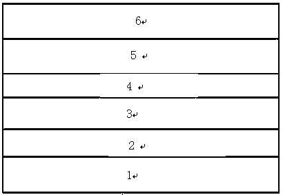
[0023] UV LED structure of the present invention, such as figure 1 As shown, it includes substrate 1, AlN buffer layer 2, n-type AlGaN layer 3, quantum well layer 4, Al z Ga 1-z N electron blocking layer 5 and p-type ohmic contact layer 6 . The p-type ohmic contact layer 6 is a diamond thin film layer. The diamond film layer is used as an ohmic contact layer structure. Because of the wide bandgap feature of the diamond film, it does not absorb the UV light emitted by the active area of the quantum well, which can greatly improve the light extraction efficiency of the UV LED.
[0024] Substrate 1 The substrate is sapphire, silicon carbide, silicon, gallium nitride, aluminum nitride or rare earth compounds. al x Ga 1-x N / Al y Ga 1-y N MQW active region 4 and Al z Ga 1-z In the N electron blocking layer 5, z>y>x.
[0025] The preparation method of above-mentioned UV LED structure, comprises the following steps:
[0026] (1) Using MOCVD (vapor phase epitaxy), MBE (mol...
PUM
 Abstract
Description
Claims
Application Information
 - R&D Engineer
- R&D Manager
- IP Professional
- Industry Leading Data Capabilities
- Powerful AI technology
- Patent DNA Extraction
Browse by: Latest US Patents, China's latest patents, Technical Efficacy Thesaurus, Application Domain, Technology Topic, Popular Technical Reports.
© 2024 PatSnap. All rights reserved.Legal|Privacy policy|Modern Slavery Act Transparency Statement|Sitemap|About US| Contact US: help@patsnap.com


