GaN-based P-type grid-enhanced type HEMT device and preparation method thereof

An enhanced, gate technology, applied in semiconductor/solid-state device manufacturing, semiconductor devices, electrical components, etc., can solve the problems of difficult to accurately control the area area, high cost, complex operation process, etc., to improve reliability, enhance Type characteristics, easy to achieve effect

Inactive Publication Date: 2016-06-08
SHANDONG INSPUR HUAGUANG OPTOELECTRONICS
View PDF6 Cites 3 Cited by
  • Summary
  • Abstract
  • Description
  • Claims
  • Application Information

AI Technical Summary

Problems solved by technology

However, the operation process of this method is complicated, it is difficult to accurately control the area, and the cost is high

Method used


Image

  • GaN-based P-type grid-enhanced type HEMT device and preparation method thereof

Examples


Embodiment Construction

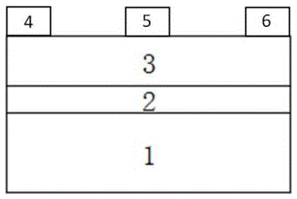
[0031] The GaN-based P-type gate enhanced HEMT device of the present invention, such as figure 1 As shown, including a substrate layer 1, a channel layer 2, a barrier layer 3, a gate 5 and a drain 6, the channel layer 2 is arranged above the substrate layer 1, and the barrier layer 3 is arranged above the channel layer 2 , the gate 5 is disposed above the barrier layer 3 , and the drain 6 is disposed on the barrier layer 3 .

[0032]The substrate layer 1 is made of silicon (Si), sapphire, silicon carbide (SiC), gallium nitride (GaN) or rare earth oxide and other materials suitable for growing III-V group compounds, and the thickness of the substrate layer 1 is 100 μm-1000 μm. The channel layer 2 is a GaN layer, and the thickness of the channel layer 2 is 0.1 μm-5 μm. The barrier layer 3 is an AlGaN layer, and the thickness of the barrier layer 3 is 0.2 μm-8 μm. The thickness of the gate 5 is 0.3nm-800nm.

[0033] The GaN-based P-type gate-enhanced HEMT device can be prepare...


PUM

PropertyMeasurementUnit
thicknessaaaaaaaaaa
thicknessaaaaaaaaaa
thicknessaaaaaaaaaa

Abstract

The invention provides a GaN-based P-type grid-enhanced type HEMT device and a preparation method thereof. The device comprises a substrate layer, a channel layer, a barrier layer, a grid electrode and a drain electrode; the channel layer is arranged on the substrate layer, the barrier layer is arranged on the channel layer, the grid electrode penetrates through the barrier layer, the drain electrode is arranged on the barrier layer, and P-type diamond is adopted as the grid electrode. The preparation method of the device comprises the following steps that 1, GaN deposition is performed on the substrate layer to form the channel layer; 2, an AlGaN layer grows on the channel layer; 3, a layer of the p-type diamond grows on the barrier layer to form the grid electrode; 4, a source electrode and the drain electrode are formed on the portions, on the two sides of the grid electrode, of the barrier layer respectively. According to the GaN-based P-type grid-enhanced type HEMT device and the preparation method thereof, the P-type diamond grid electrode is adopted, an energy band can be improved, the enhanced characteristic is achieved by using up channel electrons when the grid voltage is 0, regulation on threshold voltage of the device can be achieved, and small grid currents are kept while drain currents are increased.

Description

technical field [0001] The invention relates to a GaN-based P-type gate-enhanced HEMT (High Electron Mobility Transistor, high electron mobility transistor) device for improving ion mobility and a preparation method thereof, belonging to the technical field of semiconductors. Background technique [0002] GaN material has received more and more attention as a new type of semiconductor material. As a representative material of the third-generation semiconductor, gallium nitride has excellent electrical and optical properties. It has the advantages of wide band gap and direct band gap, high temperature and high pressure resistance, and is suitable for use in harsh environments. The main applications of gallium nitride materials are light-emitting diodes and high electron mobility transistors. Gallium nitride-based light-emitting diodes can realize wavelength changes from ultraviolet to red light, covering the entire visible light band, especially the commercialization of gall...

Claims


Application Information

Patent Timeline
Patent Type & Authority Applications(China)
IPC IPC(8): H01L29/20H01L29/43H01L21/335H01L29/778
CPCH01L29/778H01L29/2003H01L29/43H01L29/66462
Inventor 王成新逯瑶
Owner SHANDONG INSPUR HUAGUANG OPTOELECTRONICS
Why Eureka
Try Eureka