Preparation method of conductive and light transmittance perovskite quantum dot thin film
A technology of quantum dots and perovskites, which is applied in the field of preparation of conductive and light-transmitting perovskite quantum dot films, can solve the problems of difficult formation of high-precision quantum dot arrays, poor optical uniformity of conductive quantum dot films, and energy waste. It is convenient for continuous production with variable light intensity in large quantities, flexible and continuous production with variable light intensity in large quantities, and the effect of improving stability and service life
- Summary
- Abstract
- Description
- Claims
- Application Information
AI Technical Summary
Problems solved by technology
Method used
Image

Examples
Embodiment 1
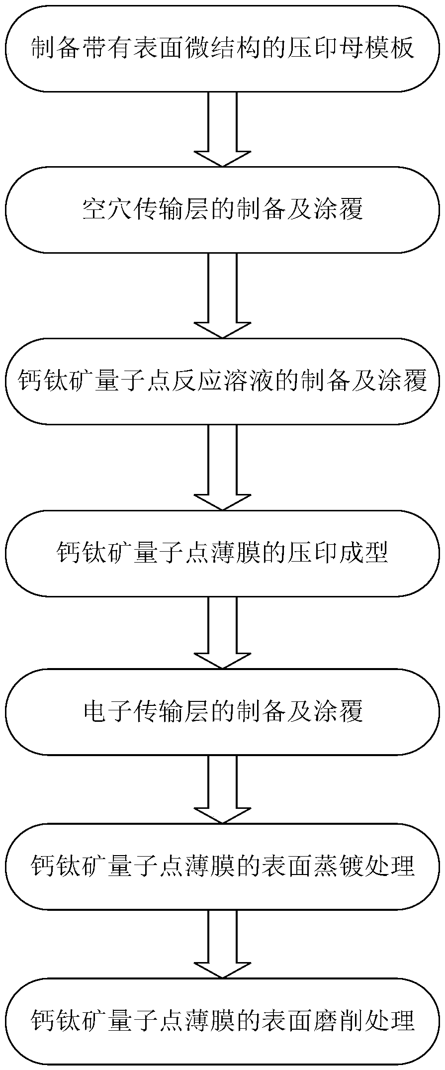
[0037] A method for preparing a conductive and light-transmitting perovskite quantum dot film, comprising the following steps:
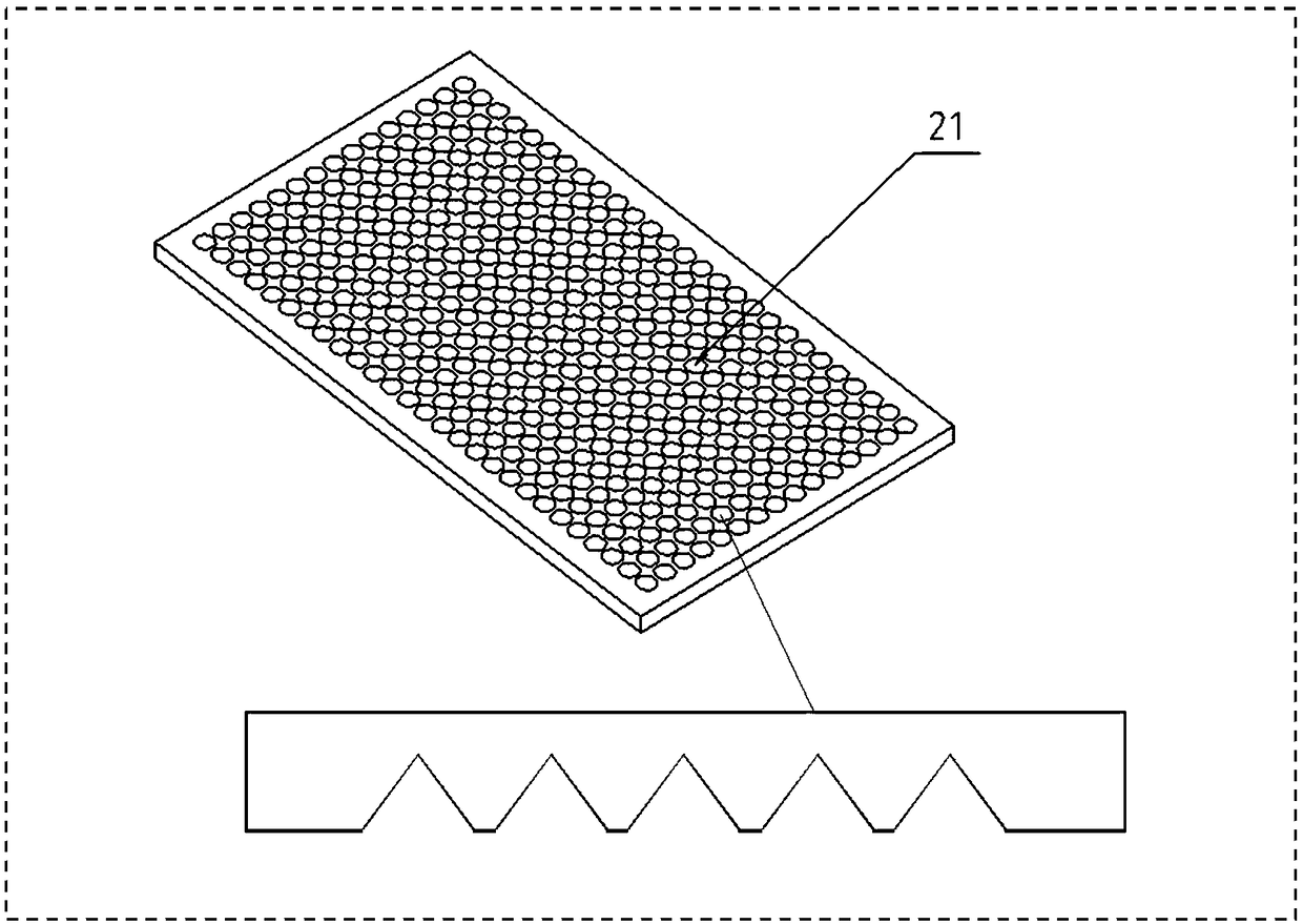
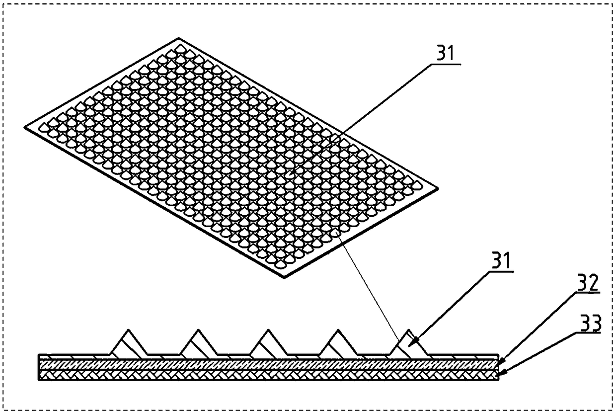
[0038] Step 1, preparation of a master template with a surface array microstructure: on a monocrystalline silicon wafer with a length of 5 cm, a width of 3 cm, and a thickness of 1 cm, ultraviolet lithography and plasma etching are used to process a master template with The master template 21 of conical hole, as the master template of surface embossing, as figure 2 As shown, the wavelength of ultraviolet light is 365nm, the power is 350W, and the power density is 30mW / cm 2 , wherein the etching gas of the plasma etching process adopts CF 4 、CH 3 F and O 2 , the cavity pressure is 50Pa, the etching power is 150W, the etching time is 2min, CH 3 The flow rate of F is 25sccm, O 2 The flow rate is 10 sccm, the diameter of the bottom surface of the conical hole is 0.2um, the height of the conical hole is 0.1um, and the distance between the central ax...
Embodiment 2
[0047] A method for preparing a conductive and light-transmitting perovskite quantum dot film, comprising the following steps:
[0048] Step 1, preparation of a master template with a surface array microstructure: on a monocrystalline silicon wafer with a length of 5 cm, a width of 3 cm, and a thickness of 1 cm, ultraviolet lithography and plasma etching are used to process a master template with The master template 21 of conical hole, as the master template of surface embossing, as figure 2 As shown, the wavelength of ultraviolet light is 360nm, the power is 340W, and the power density is 25mW / cm 2 , wherein the etching gas of the plasma etching process adopts CF 4 、CH 3 F and O 2 , the cavity pressure is 45Pa, the etching power is 140W, the etching time is 1min, CH 3 The flow rate of F is 20sccm, O 2 The flow rate is 10sccm, the diameter of the bottom surface of the conical hole is 3um, the height of the conical hole is 1.8um, and the distance between the central axes ...
Embodiment 3
[0057] A method for preparing a conductive and light-transmitting perovskite quantum dot film, comprising the following steps:
[0058] Step 1, preparation of a master template with a surface array microstructure: on a monocrystalline silicon wafer with a length of 5 cm, a width of 3 cm, and a thickness of 1 cm, ultraviolet lithography and plasma etching are used to process a master template with The master template 21 of conical hole, as the master template of surface embossing, as figure 2 As shown, the wavelength of ultraviolet light is 360nm, the power is 340W, and the power density is 25mW / cm 2 , wherein the etching gas of the plasma etching process adopts CF 4 、CH 3 F and O 2 , the cavity pressure is 55Pa, the etching power is 140W, the etching time is 1min, CH 3 The flow of F is 30sccm, O 2 The flow rate is 10 sccm, the diameter of the bottom surface of the conical hole is 5um, the height of the conical hole is 2um, and the distance between the central axes of eac...
PUM
| Property | Measurement | Unit |
|---|---|---|
| thickness | aaaaa | aaaaa |
| thickness | aaaaa | aaaaa |
| thickness | aaaaa | aaaaa |
Abstract
Description
Claims
Application Information
 - R&D
- Intellectual Property
- Life Sciences
- Materials
- Tech Scout
- Unparalleled Data Quality
- Higher Quality Content
- 60% Fewer Hallucinations
Browse by: Latest US Patents, China's latest patents, Technical Efficacy Thesaurus, Application Domain, Technology Topic, Popular Technical Reports.
© 2025 PatSnap. All rights reserved.Legal|Privacy policy|Modern Slavery Act Transparency Statement|Sitemap|About US| Contact US: help@patsnap.com