
A memory access intensive algorithm acceleration chip with multiple high speed serial memory access channels

A memory-intensive, high-speed serial technology, applied in the field of memory-intensive algorithm acceleration chips, can solve the problems of difficult interface implementation, complex system architecture design, and accelerated chip memory access bandwidth data transmission, etc. The effect of good performance, extended memory access bandwidth, and good flexibility

Inactive Publication Date: 2019-01-18
深圳市安信智控科技有限公司
View PDF4 Cites 8 Cited by
  • Summary
  • Abstract
  • Description
  • Claims
  • Application Information

AI Technical Summary

Problems solved by technology

First, the bandwidth improvement of these storage technologies is limited. They use a multi-bit parallel interface bus. The main way to further increase the bandwidth is to use a wider interface bus or increase the interface rate, but the multi-bit parallel bonded transmission requires signal integrity. It is becoming more and more difficult to implement higher, wider and higher-speed interfaces. If the main processor wants to further increase the memory access bandwidth, it must integrate more memory access interfaces, which are limited by the chip size and the number of pins. The wide bus type The number of integrated memory access interfaces is difficult to increase significantly; second, the implementation cost of new storage technologies is relatively high, for example, the engineering cost of advanced HBM technology is as high as tens of millions of dollars; third, the above-mentioned new storage technologies do not have a shared usage model , or the granularity of sharing is very low, such as DDR4 / DDR5, GDDR5, and HBM storage media can only be accessed by the main control chip directly connected to it, and cannot realize direct shared access of multiple main control chips; although HMC can connect multiple 1 main control chip, but does not support more than 4 main control chips shared use
The weak shared use characteristics of the above-mentioned various new storage technologies make the cost of adopting new storage higher to a certain extent, and limited by the storage technology, the memory access bandwidth of the algorithm acceleration chip and the data transmission between each other are also greatly affected. impact, leading to complex system architecture design

Method used


Image

  • A memory access intensive algorithm acceleration chip with multiple high speed serial memory access channels
  • A memory access intensive algorithm acceleration chip with multiple high speed serial memory access channels
  • A memory access intensive algorithm acceleration chip with multiple high speed serial memory access channels

Examples


Embodiment 1

[0032] like figure 1 As shown, a memory-intensive algorithm acceleration chip with multiple high-speed serial memory access channels includes 32 algorithm computing cores for performing data processing operations in the algorithm and 32 high-speed serial memory access channels, and also includes on-chip interconnect The network module is connected, and the algorithm calculation core and the high-speed serial memory access channel are interconnected through the on-chip interconnection network module, and the high-speed serial memory access channel is connected with an off-chip memory chip. In this embodiment, the high-speed serial access channel and the algorithm calculation core are closely coupled and connected one by one, and the 32 algorithm calculation cores are all connected to the on-chip interconnection network module. Through the on-chip interconnection network module, any algorithm calculation core can pass Any high-speed serial memory access channel accesses memory c...

Embodiment 2

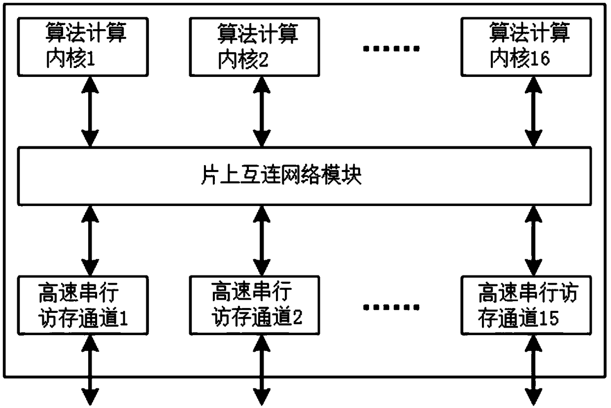
[0038] like figure 2 As shown, a memory-intensive algorithm acceleration chip with multiple high-speed serial memory access channels includes 16 algorithm computing cores for performing data processing operations in the algorithm and 15 high-speed serial memory access channels, as well as on-chip interconnect The network module is connected, and the algorithm calculation core and the high-speed serial memory access channel are interconnected through the on-chip interconnection network module, and the high-speed serial memory access channel is connected with an off-chip memory chip. In this embodiment, the high-speed serial memory access channel is loosely coupled with the algorithm calculation core, and the 16 algorithm calculation cores are all connected to the on-chip interconnection network module, and the 15 high-speed serial memory access channels are all connected to the on-chip interconnection network module. The on-chip interconnection network module, any algorithm co...


PUM


Abstract

The invention relates to the field of computer system structure and integrated circuit design, an access-intensive algorithm acceleration chip having a plurality of high-speed serial access channels is disclosed, includes a plurality of algorithm computation cores for performing data processing operations in the algorithm and a plurality of high speed serial access memory channels, the high speedserial access channel is connected with the off-chip memory chip. The implementation mode of the on-chip interconnection network module includes single bus, multi-bus, ring network, two-dimensional mesh or crossover switch. A memory access intensive algorithm acceleration chip with a plurality of high-speed serial memory access channel, the invention can flexibly expand the number of high-speed serial memory access channels according to the algorithm processing requirements so as to expand the memory access bandwidth, support various address mapping modes, and support the algorithm to accelerate the direct data transmission between chips, thus providing better flexibility for the whole machine system architecture design.

Description

technical field [0001] The invention relates to the fields of computer system structure and integrated circuit design, in particular to a memory access-intensive algorithm acceleration chip with multiple high-speed serial memory access channels. Background technique [0002] Among various types of algorithms, a large number of algorithms are memory-intensive algorithms, that is, memory access operations account for a higher proportion in the algorithm execution process, and the memory access performance largely determines the runtime performance of the algorithm. Especially for algorithms with irregular memory access patterns, that is, algorithms with poor locality of memory access, Cache (high-speed cache) cannot effectively accelerate the algorithm execution process. In this case, memory access bandwidth and latency play a decisive role in the runtime performance of the algorithm. [0003] At present, in order to improve the performance of the storage system, the industry...

Claims


Application Information

Patent Timeline
Patent Type & Authority Applications(China)
IPC IPC(8): G06F15/78G06F15/173
CPCG06F15/17368G06F15/7807
Inventor 童元满陆洪毅刘垚童乔凌
Owner 深圳市安信智控科技有限公司
Learn More