Bi-directional ESD protection device
A device and contact area technology, applied in the field of electronic science and technology, can solve problems such as reducing robustness and increasing area, and achieve the effect of improving robustness and avoiding latch-up effect.
- Summary
- Abstract
- Description
- Claims
- Application Information
AI Technical Summary
Problems solved by technology
Method used
Image
Examples
Embodiment 1
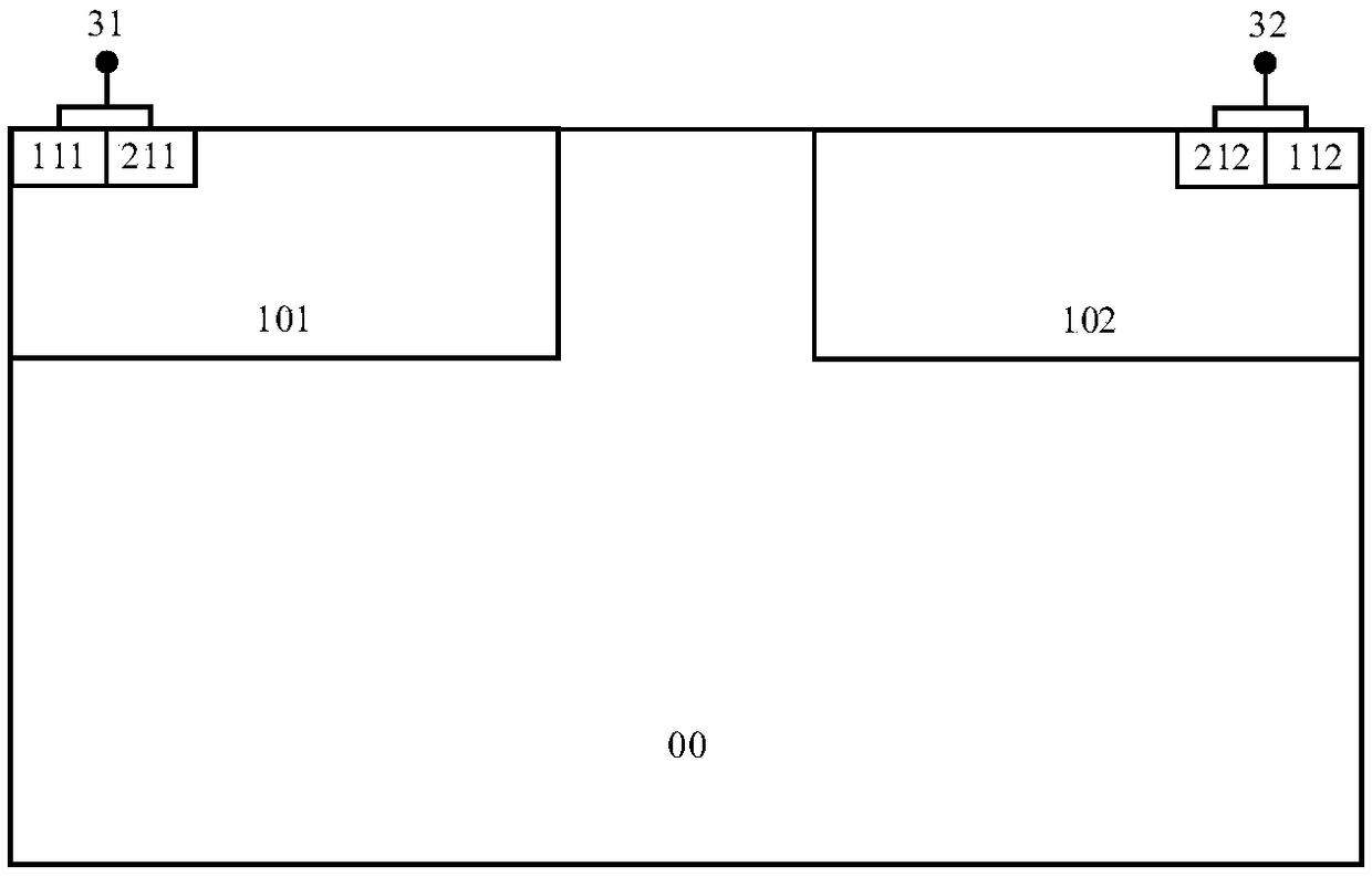
[0030] like image 3 As shown, the device structure of this embodiment includes: P-type substrate 00, N-type epitaxy 01 located above the P-type substrate, NTOP layer 13 located above the N-type epitaxy; the first PWELL located on the left side above the N-type epitaxy region 201, the first N+ contact region 111 located above the interior of the first PWELL region, the first P+ contact region 211 located above the interior of the first PWELL region, and the first NTOP layer 121 located above the interior of the first PWELL region; wherein the first The P+ contact region 211 is located on the left side of the first N+ contact region 111, the first NTOP layer 121 is located on the right side of the first N+ contact region 111; the second PWELL region 202 located on the right side above the N-type epitaxy is located above the inside of the second PWELL region The second N+ contact region 112, the second P+ contact region 212 located above the interior of the second PWELL region, ...
Embodiment 2
[0032] like Figure 4 As shown, there is an NWELL area 10 between the first PWELL area 201 and the second PWELL area 202 , and the NTOP layer 13 is located above the inside of the NWELL area 10 .
[0033] This example works as follows:
[0034] When the anode ESD voltage rises, the device first breaks down at the PN junction formed by the second PWELL region 202 / NWELL region 10 on the surface. The hole current after breakdown flows through the second PWELL region 202 and the second P+ contact region 212 , and is drawn away by the metal cathode 32 . When the current flowing through the second P+ contact region 212 increases to a certain value, so that the voltage drop between the second PWELL 202 and the second N+ contact region 112 reaches 0.7V, the parasitic NPN transistor is turned on. The second N+ contact region 112 injects electrons into the second PWELL region, and most of the electrons pass through the second NTOP layer 122 and are collected by the NWELL region 10 . ...
Embodiment 3
[0040] like Figure 5 As shown, the main difference between this embodiment and Embodiment 2 is that a first N+ low trigger area 141 is provided between the first PWELL area 201 and the NWELL area 10, and a part of the first N+ low trigger area 141 is located in the first PWELL area 201, a part is located in the NWELL area 10; a second N+ low trigger area 142 is provided between the second PWELL area 202 and the NWELL area 10, and a part of the second N+ low trigger area 142 is in the second PWELL area 202, and a part is in the Within NWELL District 10.
PUM
 Abstract
Description
Claims
Application Information
 - R&D Engineer
- R&D Manager
- IP Professional
- Industry Leading Data Capabilities
- Powerful AI technology
- Patent DNA Extraction
Browse by: Latest US Patents, China's latest patents, Technical Efficacy Thesaurus, Application Domain, Technology Topic, Popular Technical Reports.
© 2024 PatSnap. All rights reserved.Legal|Privacy policy|Modern Slavery Act Transparency Statement|Sitemap|About US| Contact US: help@patsnap.com


