A preparation method and measurement method of a pearlescent pigment cross-section sample for scanning electron microscope determination
An electron microscope and pearlescent pigment technology, which is applied in the field of pearlescent pigment materials, can solve the problems of affecting measurement, affecting authenticity, and difficulty in film thickness measurement, achieving the effect of improving reliability and simple and convenient operation
- Summary
- Abstract
- Description
- Claims
- Application Information
AI Technical Summary
Problems solved by technology
Method used
Image
Examples
Embodiment 1
[0064] Prepare the mica powder into a 10% suspended aqueous solution, adjust the pH to 2.0 with concentrated hydrochloric acid, heat and stir at 80°C, add 2mol / LTiCl4 aqueous solution to the suspension dropwise, and add NaOH solution dropwise at the same time to stabilize the pH value at 2, after 15 minutes Stop adding the TiCl4 aqueous solution, and the pH value of the reaction system rises to 8.5; slowly add a certain amount of tetraethyl orthosilicate solution to the reaction system dropwise, and keep the pH of the reaction solution stable at 8.5±0.2. The pH of the solution was adjusted to 2.0, and TiCl was added dropwise to the reaction system again 4 Aqueous solution, stop adding after 10 minutes, settle, filter with suction, wash with water, and dry to obtain mica titanium pearlescent pigment.
Embodiment 2
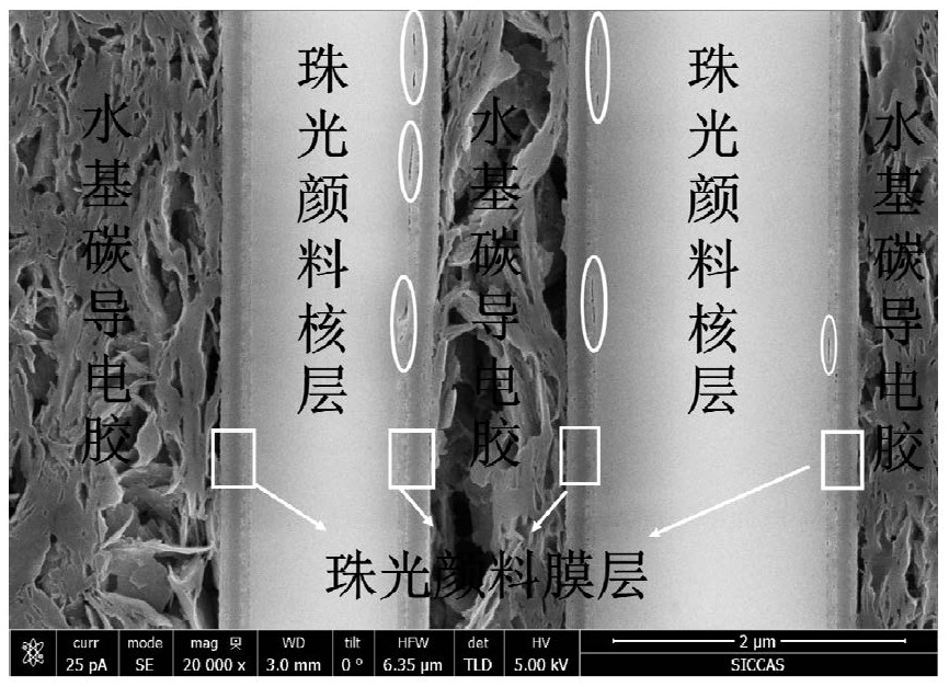
[0066] First, the pearlescent pigment is fixed on the surface of a silicon wafer (0.2mm) by the above method, and the initial sample with the pearlescent pigment coating layer fixed is obtained after drying. The mass ratio of the water-based liquid carbon conductive adhesive to the pearlescent pigment is 1:5 , the thickness of the fixed pearlescent pigment is 1mm. First load the sample stage with the initial sample into the argon ion beam polisher, and make the side of the silicon wafer not coated with pearlescent pigments close to the baffle, so that the ion beam first breaks down the silicon wafer, and then It is polished with pearlescent pigments. Among them, the parameters of ion beam section polishing include: acceleration voltage: 5kV, current: 2mA, polishing time: 4h. Secondly, use a scanning electron microscope to observe the pearlescent pigment section sample after ion beam section polishing, select a magnification of 40,000 times, voltage: 5kV, current: 25pA, to obt...
Embodiment 3
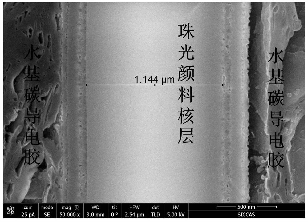
[0068] First, the pearlescent pigment is fixed on the surface of a silicon wafer (0.2mm) by the above method, and the initial sample with the pearlescent pigment coating layer fixed is obtained after drying. The mass ratio of the water-based liquid carbon conductive adhesive to the pearlescent pigment is 1:5 , the thickness of the fixed pearlescent pigment is 1mm. First load the sample stage with the initial sample into the argon ion beam polisher, and make the side of the silicon wafer not coated with pearlescent pigments close to the baffle, so that the ion beam first breaks down the silicon wafer, and then It is polished with pearlescent pigments. Among them, the parameters of ion beam section polishing include: acceleration voltage: 5kV, current: 2mA, polishing time: 4h. Secondly, select one of the pearlescent pigment cross-sections and select a magnification of 50,000 times, voltage: 5kV, current: 25pA, to obtain a clear secondary electron image, see the attached figur...
PUM
| Property | Measurement | Unit |
|---|---|---|
| thickness | aaaaa | aaaaa |
| thickness | aaaaa | aaaaa |
| thickness | aaaaa | aaaaa |
Abstract
Description
Claims
Application Information
 - Generate Ideas
- Intellectual Property
- Life Sciences
- Materials
- Tech Scout
- Unparalleled Data Quality
- Higher Quality Content
- 60% Fewer Hallucinations
Browse by: Latest US Patents, China's latest patents, Technical Efficacy Thesaurus, Application Domain, Technology Topic, Popular Technical Reports.
© 2025 PatSnap. All rights reserved.Legal|Privacy policy|Modern Slavery Act Transparency Statement|Sitemap|About US| Contact US: help@patsnap.com


