Single-chip integrated tunnel junction laser for microwave oscillation source
A microwave oscillation source and monolithic integration technology, which is applied to lasers, laser components, semiconductor lasers, etc., can solve the problems of low modulation rate of microwave oscillation sources, high power loss, and high phase noise, so as to reduce phase noise and reduce Effects of power loss, high-speed modulation
- Summary
- Abstract
- Description
- Claims
- Application Information
AI Technical Summary
Problems solved by technology
Method used
Image
Examples
Embodiment 1
[0041] Embodiment 1 is a monolithic integrated tunnel junction laser for a microwave oscillation source with a lasing wavelength near 1.55 μm.
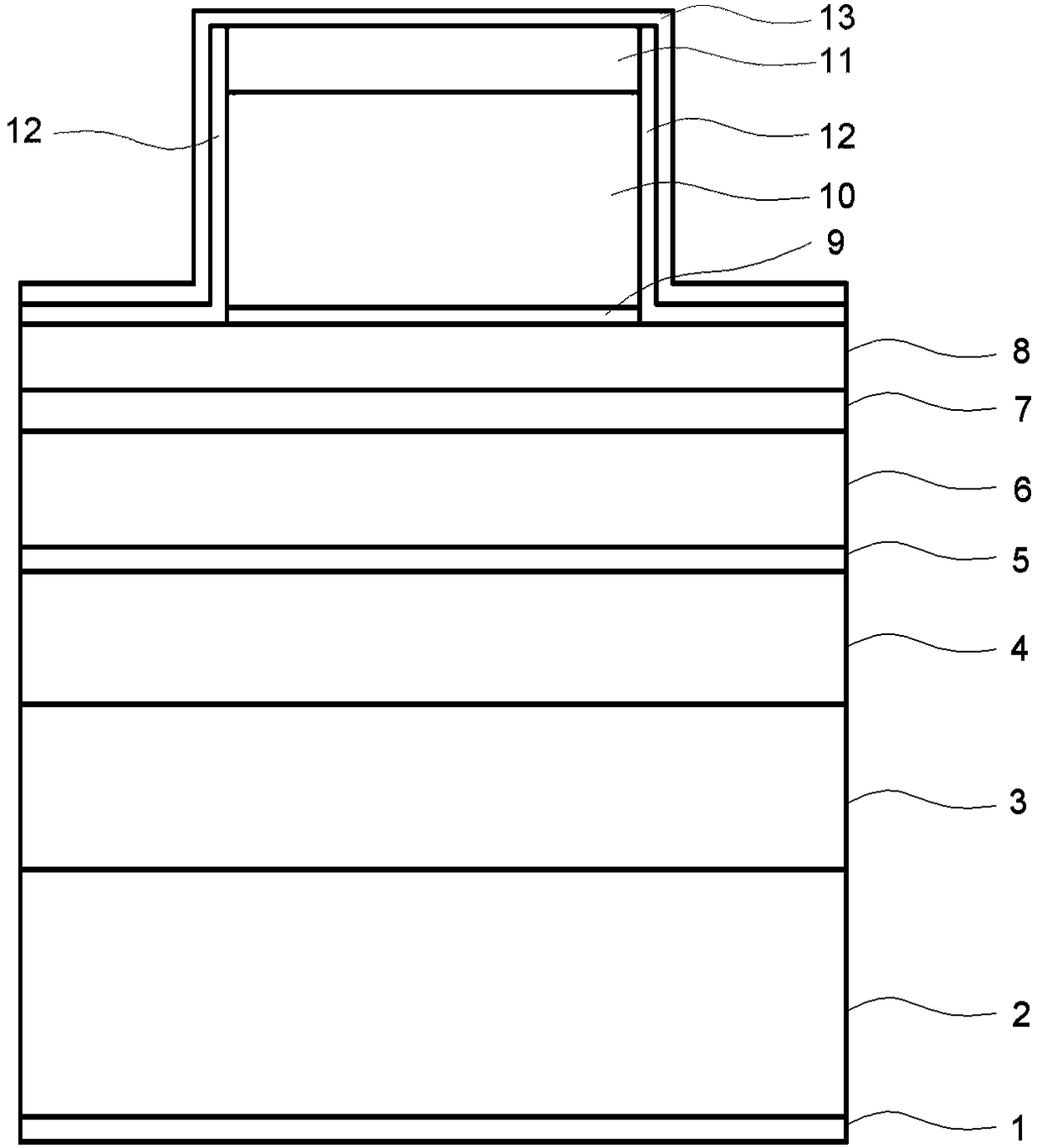
[0042] Such as figure 1 As shown, the monolithic integrated tunnel junction laser for microwave oscillation source in embodiment 1, from bottom to top, is N electrode 1, N-type InP substrate 2, N-type InP buffer layer 3, lower confinement layer 4, quantum Well active region 5 , upper confinement layer 6 , grating layer 7 , N-type InP layer 8 , tunnel junction 9 , P-type InP capping layer 10 , P-type contact layer 11 , insulating isolation layer 12 and P-electrode 13 .
[0043] N electrode 1, N-type InP substrate 2, N-type InP buffer layer 3, lower confinement layer 4, quantum well active region 5, upper confinement layer 6, grating layer 7, and N-type InP layer 8 have the same width; N Type InP layer 8 is a ridge waveguide structure formed by tunnel junction 9, P-type InP capping layer 10 and P-type contact layer 11. The width of the...
Embodiment 2
[0056] Embodiment 2 is a monolithic integrated tunnel junction laser for a microwave oscillation source with a lasing wavelength near 1.31 μm.
[0057] Such as figure 1 As shown, the monolithic integrated tunnel junction laser used for microwave oscillation source in embodiment 2 is N electrode 1, N-type InP substrate 2, N-type InP buffer layer 3, lower confinement layer 4, quantum Well active region 5 , upper confinement layer 6 , grating layer 7 , N-type InP layer 8 , tunnel junction 9 , P-type InP capping layer 10 , P-type contact layer 11 , insulating isolation layer 12 and P-electrode 13 .
[0058] N electrode 1, N-type InP substrate 2, N-type InP buffer layer 3, lower confinement layer 4, quantum well active region 5, upper confinement layer 6, grating layer 7, and N-type InP layer 8 have the same width; N Type InP layer 8 is a ridge waveguide structure formed by tunnel junction 9, P-type InP capping layer 10 and P-type contact layer 11. The width of the ridge waveguide...
PUM
 Abstract
Description
Claims
Application Information
 - R&D Engineer
- R&D Manager
- IP Professional
- Industry Leading Data Capabilities
- Powerful AI technology
- Patent DNA Extraction
Browse by: Latest US Patents, China's latest patents, Technical Efficacy Thesaurus, Application Domain, Technology Topic, Popular Technical Reports.
© 2024 PatSnap. All rights reserved.Legal|Privacy policy|Modern Slavery Act Transparency Statement|Sitemap|About US| Contact US: help@patsnap.com


