A controllable multi-wavelength fiber external cavity laser based on super-surface external cavity mirror
A metasurface and multi-wavelength technology, applied in the laser field, can solve problems such as unsatisfactory output wavelength stability and complex structure of multi-wavelength lasers, and achieve controllable and stable output, low cost, and stable output.
- Summary
- Abstract
- Description
- Claims
- Application Information
AI Technical Summary
Problems solved by technology
Method used
Image
Examples
Embodiment 1
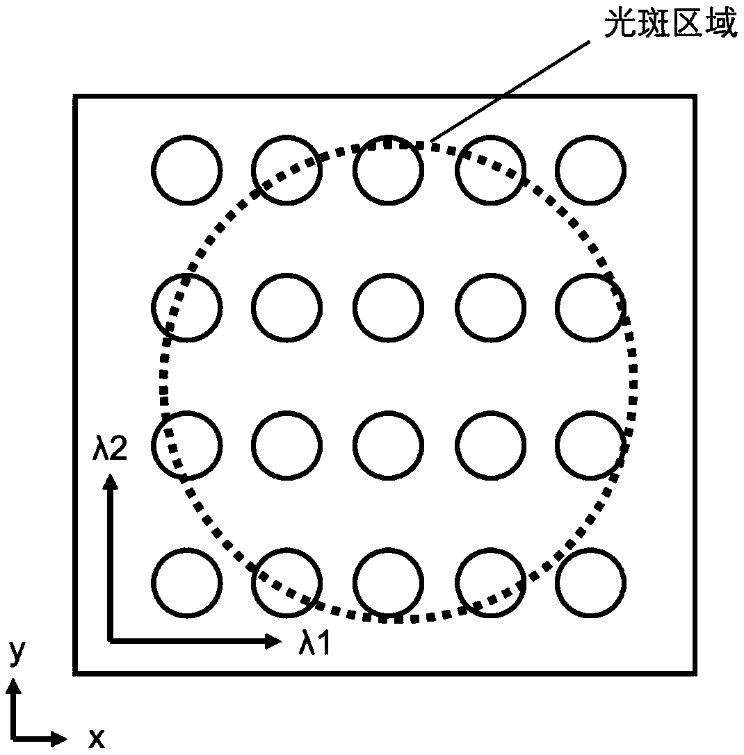
[0043] This embodiment is a dual-wavelength fiber external cavity laser.
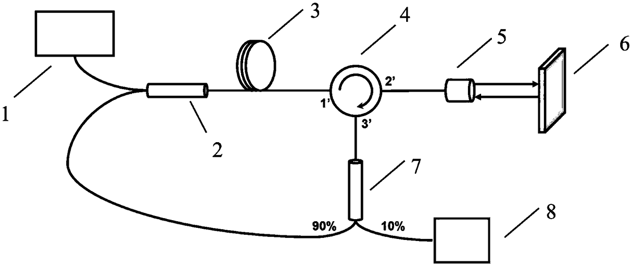
[0044] Such as figure 1 As shown, the controllable multi-wavelength fiber external cavity laser based on the metasurface external cavity mirror includes: fiber amplifier, fiber circulator 4, fiber collimator 5, metasurface external cavity mirror 6 and fiber coupler 7, wherein,
[0045] A fiber amplifier, a fiber circulator 4, a fiber collimator 5, a metasurface external cavity mirror 6 and a fiber coupler 7 are sequentially arranged to form a ring cavity structure.
[0046] In this embodiment, the optical fiber amplifier is preferably composed of a 980nm pump source 1, a 980nm / 1550nm wavelength division multiplexer 2 and an erbium-doped fiber 3; the gain range of the erbium-doped fiber 3 is preferably 1530nm to 1570nm, and the length is 20m; The working range of the fiber circulator 4 , the fiber collimator 5 and the fiber coupler 7 is preferably 1530 nm to 1580 nm; the fiber coupler 7 is preferably a ...
Embodiment 2
[0054] This embodiment is a four-wavelength fiber external cavity laser.
[0055] The structure of the laser in this embodiment is the same as that in Embodiment 1, the difference is that the pattern structure of the metasurface of the metasurface external cavity mirror 6 in this embodiment is different, and it adopts a pattern structure of a four-wavelength reflective metasurface.
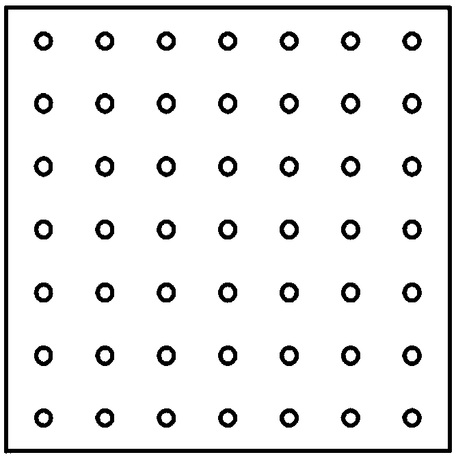
[0056] Such as Figure 4 As shown, it is a schematic diagram of a four-wavelength reflective metasurface structure. The metasurface structure is composed of four nanohole arrays (micro-nano pattern arrays) with different reflection wavelengths. The spot of collimated light is located in the central area of the metasurface structure. . The SOI substrate with a top silicon thickness of 220nm is etched by micro-nano processing techniques such as electron beam exposure and etching. Figure 4 The four-wavelength reflective metasurface structure shown. The structure is closely spliced by four nan...
PUM
 Abstract
Description
Claims
Application Information
 - R&D Engineer
- R&D Manager
- IP Professional
- Industry Leading Data Capabilities
- Powerful AI technology
- Patent DNA Extraction
Browse by: Latest US Patents, China's latest patents, Technical Efficacy Thesaurus, Application Domain, Technology Topic, Popular Technical Reports.
© 2024 PatSnap. All rights reserved.Legal|Privacy policy|Modern Slavery Act Transparency Statement|Sitemap|About US| Contact US: help@patsnap.com


