A processing method for improving three-dimensional micro-nano structures based on composite scanning
A processing method and technology of micro-nano structure, which are applied in the direction of photo-engraving process, micro-lithography exposure equipment, photo-engraving process exposure device, etc. on the pattern surface, which can solve the problems of slow response time, difficult to process three-dimensional structure, difficult to satisfy and so on. , to improve the width accuracy, reduce the width error and improve the smoothness
- Summary
- Abstract
- Description
- Claims
- Application Information
AI Technical Summary
Problems solved by technology
Method used
Image
Examples
Embodiment
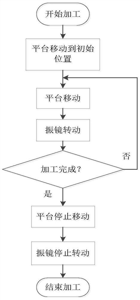
[0033] This embodiment discloses a processing method for improving a three-dimensional micro-nano structure based on composite scanning, including the following steps:
[0034] S1, coating photoresist on the substrate;
[0035] S2. Adjust the optical signal emitted by the laser light source according to the exposure requirements of the photoresist, including beam expansion, polarization adjustment, phase adjustment, light intensity adjustment, etc.;
[0036] S3. Pass the adjusted laser beam through the two-dimensional vibrating mirror first, and then focus on the specified position in the photoresist through the objective lens;
[0037] S4. Split the three-dimensional structural model to be processed into several two-dimensional planes along the longitudinal axis, and each two-dimensional plane figure is filled and fitted by several points;
[0038] S5. Import the spatial coordinate information of all the points combined into the three-dimensional model structure into the pro...
Embodiment 2
[0053] In this embodiment, according to the processing method of improving the three-dimensional micro-nano structure based on compound scanning of the present invention, the specific implementation steps of preparing a structure composed of lines in the photoresist with the trade name SZ2080 are described in detail:
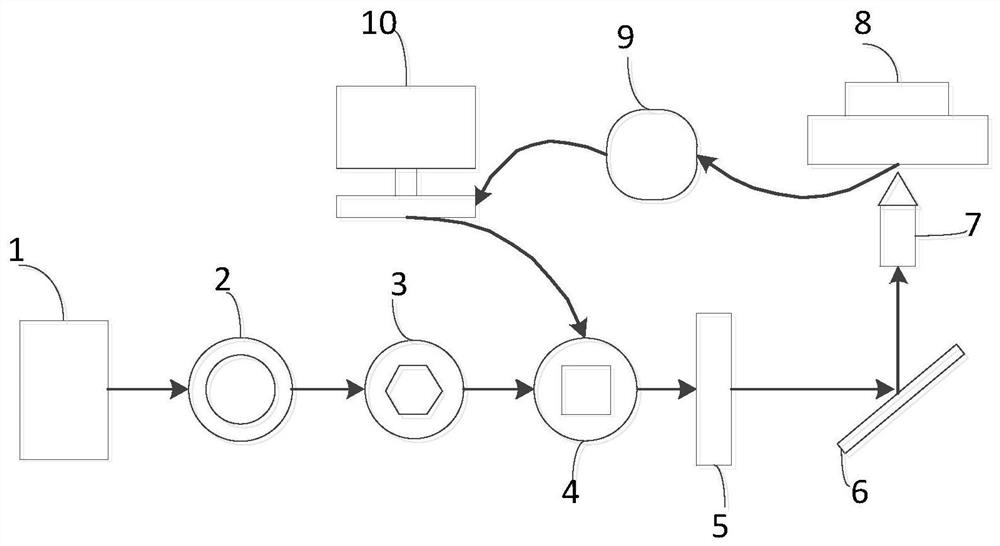
[0054] (1) The processing equipment used in this embodiment is as figure 1 As shown, the device marked 1 in the figure represents a femtosecond pulse laser, which emits laser pulses with a wavelength of 532nm. The laser beam is emitted from the laser and passes through a 1 / 2 wave plate used to adjust the light intensity, marked as 2 in the figure. Then the laser beam passes through an aperture (No. 3) and a shutter (No. 4) to reach the front of the two-dimensional vibrating mirror (No. 5). Then the laser beam passes through the vibrating mirror and enters the objective lens vertically placed under the three-dimensional platform through a reflector (No. 7). Fi...
PUM
| Property | Measurement | Unit |
|---|---|---|
| wavelength | aaaaa | aaaaa |
Abstract
Description
Claims
Application Information
 - R&D
- Intellectual Property
- Life Sciences
- Materials
- Tech Scout
- Unparalleled Data Quality
- Higher Quality Content
- 60% Fewer Hallucinations
Browse by: Latest US Patents, China's latest patents, Technical Efficacy Thesaurus, Application Domain, Technology Topic, Popular Technical Reports.
© 2025 PatSnap. All rights reserved.Legal|Privacy policy|Modern Slavery Act Transparency Statement|Sitemap|About US| Contact US: help@patsnap.com


