Homogenous PN (positive-negative) junction on basis of two-dimensional semiconductor materials and method for preparing homogenous PN junction
A two-dimensional semiconductor, semiconductor technology, applied in the field of nanoelectronics
- Summary
- Abstract
- Description
- Claims
- Application Information
AI Technical Summary
Problems solved by technology
Method used
Image
Examples
Embodiment Construction
[0036] The present invention will be further described through the embodiments below in conjunction with the accompanying drawings.
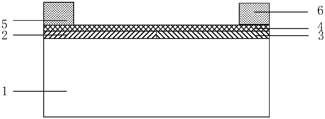
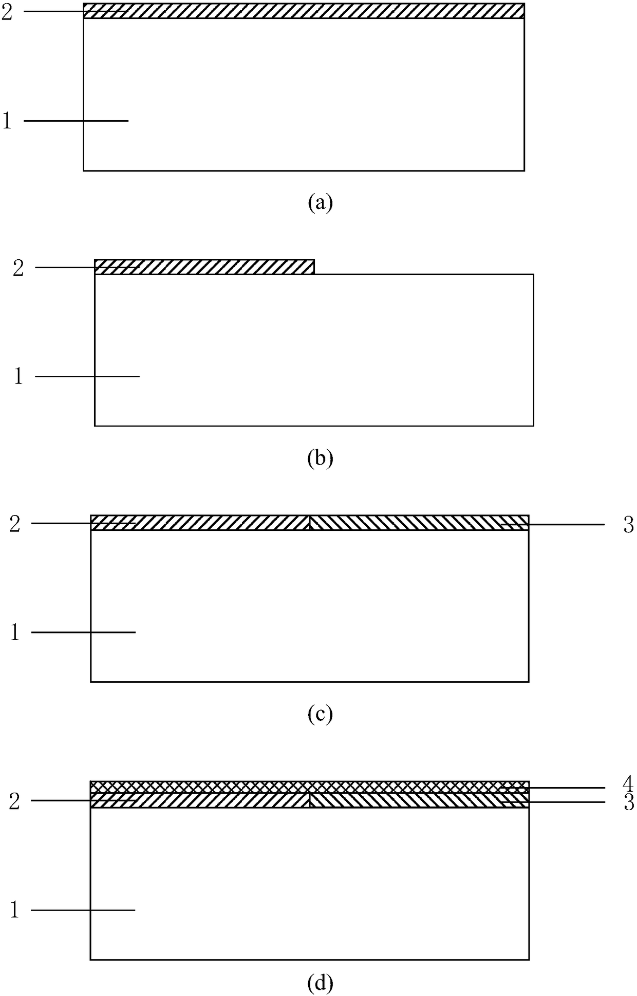
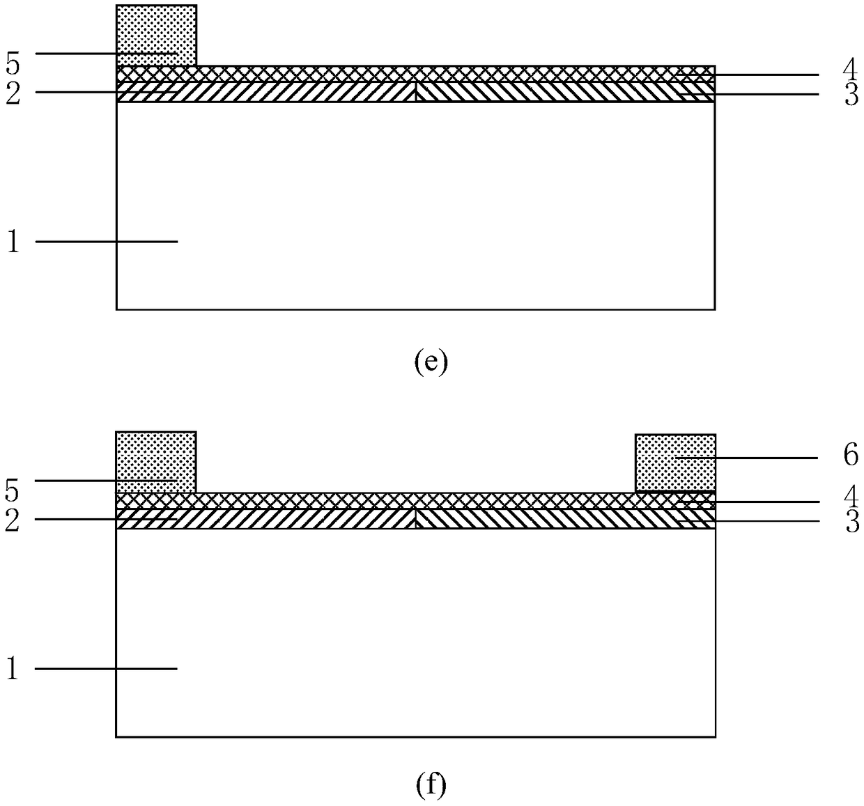
[0037] like figure 1As shown, the prepared homogeneous PN junction based on two-dimensional semiconductor materials includes an insulating substrate 1, a first two-dimensional semiconductor material 2, a second two-dimensional semiconductor material 3, a third two-dimensional semiconductor material 4, and a P-type region metal Contact electrode 5 and N-type regional metal contact electrode 6 . Wherein, the first two-dimensional semiconductor material 2 and the second two-dimensional semiconductor material 3 are located on the insulating substrate 1, the third two-dimensional semiconductor material 4 is located above the first two-dimensional semiconductor material 2 and the second two-dimensional semiconductor material 3, P The type region metal contact electrode 5 and the N type region metal contact electrode 6 are respectively located on the ...
PUM
| Property | Measurement | Unit |
|---|---|---|
| Thickness | aaaaa | aaaaa |
Abstract
Description
Claims
Application Information
 - R&D
- Intellectual Property
- Life Sciences
- Materials
- Tech Scout
- Unparalleled Data Quality
- Higher Quality Content
- 60% Fewer Hallucinations
Browse by: Latest US Patents, China's latest patents, Technical Efficacy Thesaurus, Application Domain, Technology Topic, Popular Technical Reports.
© 2025 PatSnap. All rights reserved.Legal|Privacy policy|Modern Slavery Act Transparency Statement|Sitemap|About US| Contact US: help@patsnap.com


