On-chip test DC probe card

A probe card, feeding probe technology, applied in semiconductor/solid-state device testing/measurement, electrical components, circuits, etc., can solve the problem of affecting microwave chip test results, cost and process are difficult to achieve, and the DC oscillation of the chip to be tested and other problems to achieve the effect of improving test performance, simple structure and low cost

Inactive Publication Date: 2018-11-06
NO 55 INST CHINA ELECTRONIC SCI & TECHNOLOGYGROUP CO LTD
View PDF6 Cites 2 Cited by
  • Summary
  • Abstract
  • Description
  • Claims
  • Application Information

AI Technical Summary

Problems solved by technology

[0003] At present, microwave integrated circuit chips are mostly tested using various microwave test instruments and probe stations. The DC feed of the chip to be tested generally uses a DC probe to contact the DC feed point of the chip, but the clutter of the bias power supply is also It will be loaded on the chip under test through the bias loop, which will affect the test results of the microwave chip
It is difficult to realize the bypass capacitor with a large area inside the chip in terms of cost and process. If the DC probe is accurately modeled and the influence of the embedded DC probe on the microwave test result is removed during the test, this The method requires huge manpower and material resources, which is impractical
Especially for the test of amplifier chips, due to the parasitic effect of traditional DC probes, it is easy to cause DC oscillation of the chip under test, which often leads to failure to test

Method used


Image

  • On-chip test DC probe card
  • On-chip test DC probe card
  • On-chip test DC probe card

Examples


Embodiment Construction

[0015] The technical solutions of the present invention will be further described below in conjunction with the accompanying drawings and embodiments.

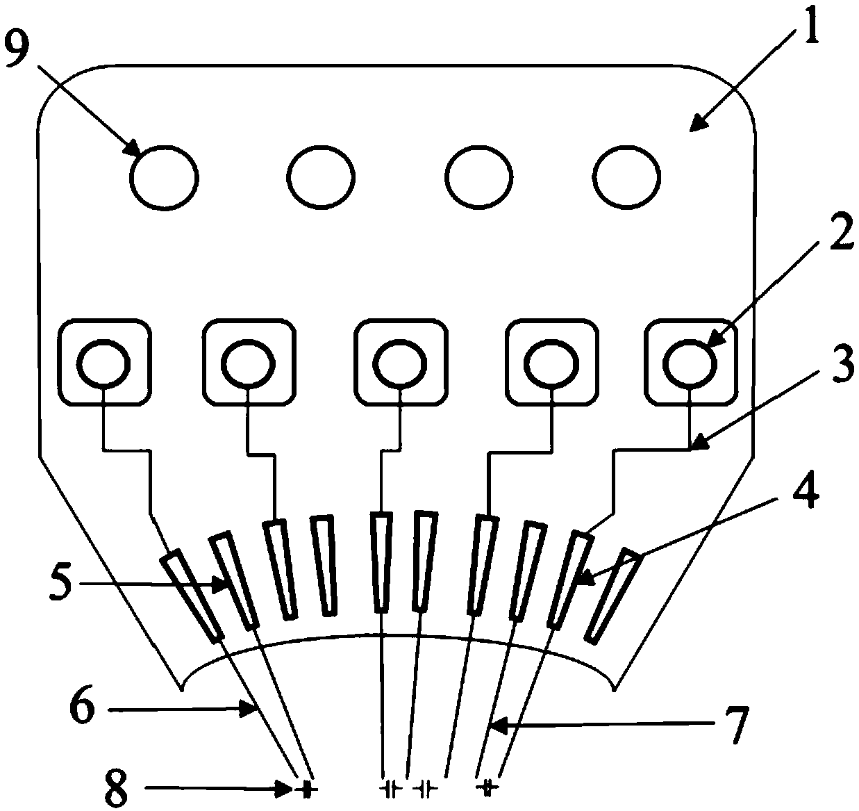
[0016] like figure 1 As shown, the on-chip test DC probe card of the present invention includes an annular dielectric substrate 1, the upper surface of the annular dielectric substrate 1 is attached with an SMB connector 2, a needle element position for welding the SMB connector 2, a DC feeder 3, a welding The DC feed pad 4 of the DC feed probe, the ground pad 5 of the ground probe, the DC feed probe 6 and the ground probe 7 are welded.

[0017] The SMB connector 2 is connected to the power supply through a cable, and then correspondingly connected to the DC feed pad 4 through the DC feed line 3. The DC feed probe 6 is welded on the corresponding DC feed pad 4 on the annular dielectric substrate 1. The DC feed The needle tip of the electric probe 6 is connected with the chip to be tested through the feed voltage block.

[00...


PUM

PropertyMeasurementUnit
Capacitanceaaaaaaaaaa

Abstract

The invention discloses an on-chip test DC probe card, and aims at overcoming the defect a traditional DC probe card has a parasitic inductance effect and meeting on-chip test requirements of different microwave monolithic integrated circuits. The on-chip test DC probe card comprises an annular dielectric substrate, DC feed and grounding probes are welded to the upper surface of the substrate, a capacitor is connected to the probes, the DC feed probe is connected with the upper electrode of the capacitor, the grounding probe is connected with the lower electrode of the capacitor, the feed probe is connected to a DC voltage block of a tested chip via the upper electrode of the capacitor, and the grounding problem is connected to a grounding voltage block of the tested chip via the lower electrode of the capacitor. Thus, traditional influence of the DC probe on a test result of the microwave chip is eliminated, and the test performance is improved.

Description

technical field [0001] The invention relates to the field of microwave on-chip testing, in particular to a DC probe card for on-chip testing. Background technique [0002] Microwave on-chip testing is to perform a functional test on the bare chip with a probe before the microwave monolithic integrated circuit is packaged, to screen out defective products, and then proceed to the subsequent packaging project. In short, the on-wafer test DC probe card is the interface between the test machine and the wafer. Each test component requires at least one corresponding DC probe card, and the purpose of the test is to make the wafer good after dicing. Enter the next packaging process, and avoid waste caused by continued processing of defective products. Therefore, the impact of DC probe cards on manufacturing costs and test results in integrated circuit manufacturing is very important. [0003] At present, microwave integrated circuit chips are mostly tested using various microwave ...

Claims


Application Information

Patent Timeline
IPC IPC(8): H01L21/66
CPCH01L22/30
Inventor 洪希依陈金远章军云黄念宁
Owner NO 55 INST CHINA ELECTRONIC SCI & TECHNOLOGYGROUP CO LTD
Why Eureka
Try Eureka