


Quick Research
Generate reliable direction feasibility study reports for your R&D in just a few steps.

Technical Q&A
Discover and master advanced knowledge NOW. Basics, ideas, possibilities, all at once.

Find Solutions
As an expert in R&D theories, this can generate solutions to your technical problems instantly.

Evaluate Feasibility
Analyze your overall solution with one click, know your potential R&D risks in advance.

Monitor Landscape
Get weekly tech updates, stay abreast of the latest tech innovations and key insights.
Semiconductor device, receiving device, and transmitting device
A technology for transmitting devices and semiconductors, which is applied in the field of receiving devices, transmitting devices, and semiconductor devices, and can solve problems such as signal processing performance degradation of signal processing circuits, and achieve the effect of reducing the influence of parasitic inductance
- Summary
- Abstract
- Description
- Claims
- Application Information
AI Technical Summary
Problems solved by technology
Method used
Image

Examples
no. 1 Embodiment approach
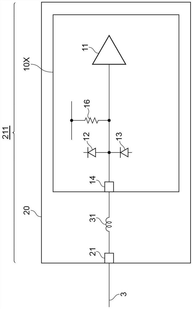
[0053] Figure 5 It is a figure which shows the structure of the semiconductor device 111 of 1st Embodiment. The semiconductor device 111 includes a semiconductor chip 10A and a package 20 , and receives a signal transmitted through the signal transmission path 3 .
[0054] A semiconductor chip (10A) has a signal processing circuit 11, ESD protection elements 12, 13, a plurality of pads, and a first resistor 16, which are formed in or on a semiconductor substrate. On the semiconductor chip 10A, among the plurality of pads, the first pad 14 and the second pad 15 are not shorted to each other. The signal input terminal of the signal processing circuit 11 is connected to the second pad 15 . The ESD protection element 12 is provided between a reference potential supply terminal for supplying a power supply potential and the first pad 14 . The ESD protection element 13 is provided between a reference potential supply terminal for supplying a ground potential and the first pad 14...
no. 2 Embodiment approach
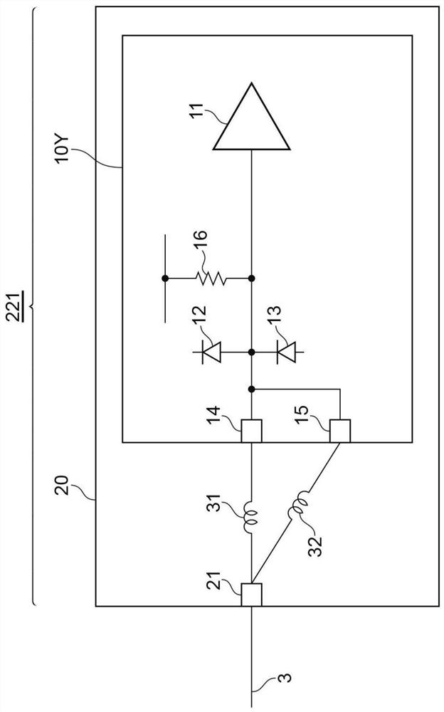
[0076] Figure 8 It is a figure which shows the structure of the semiconductor device 121 of 2nd Embodiment. This semiconductor device 121 includes a semiconductor chip 10B and a package 20 , and receives a signal transmitted through the signal transmission path 3 . Compared with the semiconductor chip 10A of the first embodiment, the semiconductor chip 10B of the second embodiment is different in that it further includes a second resistor 17 . The second resistor 17 is provided between a reference potential supply terminal for supplying a power supply potential and the second pad 15 .
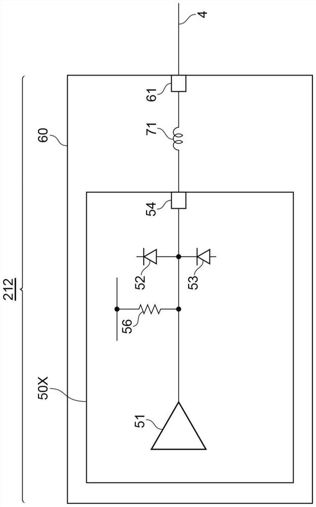
[0077] Figure 9 It is a figure which shows the structure of the semiconductor device 122 of 2nd Embodiment. This semiconductor device 122 includes a semiconductor chip 50B and a package 60 , and transmits a signal to the signal transmission line 4 . Compared with the semiconductor chip 50A in the first embodiment, the semiconductor chip 50B in the second embodiment is different in that it...
no. 3 Embodiment approach
[0082] Figure 10 It is a figure which shows the structure of the semiconductor device 131 of 3rd Embodiment. This semiconductor device 131 includes a semiconductor chip 10C and a package 20 , and receives a signal transmitted through the signal transmission path 3 . Compared with the semiconductor chip 10A of the first embodiment, the semiconductor chip 10C of the third embodiment is different in that it further includes a third resistor 18 . The third resistor 18 is provided between the first pad 14 and the second pad 15 .
[0083] Figure 11 It is a figure which shows the structure of the semiconductor device 132 of 3rd Embodiment. This semiconductor device 132 includes a semiconductor chip 50C and a package 60 , and transmits a signal to the signal transmission line 4 . Compared with the semiconductor chip 50A of the first embodiment, the semiconductor chip 50C of the third embodiment is different in that it further includes a third resistor 58 . The third resistor 58...
PUM
| Property | Measurement | Unit |
|---|---|---|
| frequency | aaaaa | aaaaa |
| impedance | aaaaa | aaaaa |
| electrical resistance | aaaaa | aaaaa |
Abstract
Description
Claims
Application Information
 - R&D Engineer
- R&D Manager
- IP Professional
- Industry Leading Data Capabilities
- Powerful AI technology
- Patent DNA Extraction
Browse by: Latest US Patents, China's latest patents, Technical Efficacy Thesaurus, Application Domain, Technology Topic, Popular Technical Reports.
© 2024 PatSnap. All rights reserved.Legal|Privacy policy|Modern Slavery Act Transparency Statement|Sitemap|About US| Contact US: help@patsnap.com