


Quick Research
Generate reliable direction feasibility study reports for your R&D in just a few steps.

Technical Q&A
Discover and master advanced knowledge NOW. Basics, ideas, possibilities, all at once.

Find Solutions
As an expert in R&D theories, this can generate solutions to your technical problems instantly.

Evaluate Feasibility
Analyze your overall solution with one click, know your potential R&D risks in advance.

Monitor Landscape
Get weekly tech updates, stay abreast of the latest tech innovations and key insights.
A high-speed semiconductor laser and its packaging structure and method
A packaging structure and laser technology, which is applied in the direction of semiconductor lasers, lasers, laser components, etc., can solve the problems of lower device reliability, lower laser working speed, serious laser heating, etc., to improve yield and laser flip-chip welding is reliable Effect
- Summary
- Abstract
- Description
- Claims
- Application Information
AI Technical Summary
Problems solved by technology
Method used
Image

Examples
Embodiment 1
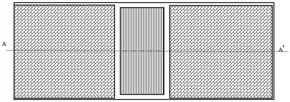
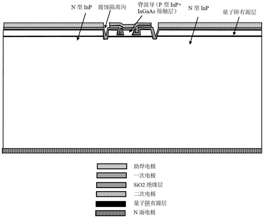
[0041] see Figure 1 to Figure 3 , an embodiment of the present invention provides a high-speed semiconductor laser, including an N-type substrate, an epitaxial structure is grown on the upper surface of the N-type substrate, an insulating layer is deposited after etching a ridge waveguide on the upper surface of the N-type substrate, and the two sides of the ridge waveguide are The sides of the ridge waveguide are grooves, and the grooves on both sides of the ridge waveguide are also covered with an insulating layer. Only the insulating layer on the upper surface of the ridge waveguide is removed, and a P-type electrode is deposited on the upper surface of the ridge waveguide; the lower surface of the N-type substrate is provided with an N-type electrode.
[0042] When depositing the P-type electrode, the P-type electrode can only cover the upper surface area of the ridge waveguide. Of course, when depositing the P-type electrode, the deposition area of the P-type electrode...
Embodiment 2
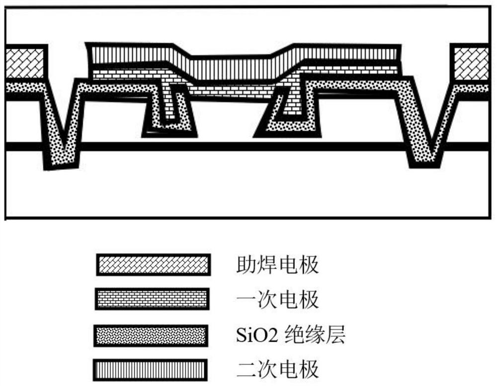
[0053] see Figure 5 to Figure 8 , an embodiment of the present invention provides a high-speed semiconductor laser packaging structure, including a semiconductor laser and a heat sink, the upper surface of the heat sink is provided with a P-type transition electrode, the semiconductor laser is flip-chip on the heat sink, and the P of the semiconductor laser is The P-type electrode faces down, and is soldered to the P-type transition electrode on the upper surface of the heat sink through solder. The P-type transition electrode on the heat sink extends beyond the laser, and the extension of the P-type transition electrode beyond the laser corresponds to the package on the tube base The pins are electrically connected, and the extension of the P-type transition electrode beyond the laser can be connected with the corresponding package pin on the tube base through a gold wire lead, or can be directly welded.
[0054] Further, the light-emitting end surface of the laser protrudes...
Embodiment 3
[0062] see Figure 5 to Figure 8 , an embodiment of the present invention provides a high-speed semiconductor laser flip-chip packaging method,
[0063] Including the following steps:
[0064] Making the semiconductor laser described in Embodiment 1;
[0065] The manufacturing steps of the semiconductor laser include: growing a buffer layer on an N-type InP substrate, a quantum well active region, and a P-type InP confinement layer and a P-type InGaAs contact layer. In the process preparation, it is necessary to etch out the light-emitting strip in the active area with a width of approximately 2um, then deposit an insulating layer, remove the insulating layer on the light-emitting strip, and then deposit a P-type electrode. After the substrate is thinned to approximately ~100um, an N-type electrode is deposited on the N surface, and then the laser is cut into cuboids with a cavity length of 150-500um, a width of ~250um, and a thickness of ~100um by cleavage and cleavage. Bo...
PUM
 Abstract
Description
Claims
Application Information
 - R&D Engineer
- R&D Manager
- IP Professional
- Industry Leading Data Capabilities
- Powerful AI technology
- Patent DNA Extraction
Browse by: Latest US Patents, China's latest patents, Technical Efficacy Thesaurus, Application Domain, Technology Topic, Popular Technical Reports.
© 2024 PatSnap. All rights reserved.Legal|Privacy policy|Modern Slavery Act Transparency Statement|Sitemap|About US| Contact US: help@patsnap.com